MOSFET – N-Channel,
SUPERFET II, FRFET
650 V, 54 A, 77 mW
FCH077N65F
Description
SUPERFET® II MOSFET is ON Semiconductor’s brand−new high
voltage super−junction (SJ) MOSFET family that is utilizing charge
balance technology for outstanding low on−resistance and lower gate
charge performance. This technology is tailored to minimize
conduction loss, provide superior switching performance, dv/dt rate
and higher avalanche energy. Consequently, SUPERFET II MOSFET
is very suitable for the switching power applications such as PFC,
server/telecom power, FPD TV power, ATX power and industrial
power applications. SUPERFET II FRFET® MOSFET’s optimized
body diode reverse recovery performance can remove additional
component and improve system reliability.
www.onsemi.com
VDS
RDS(ON) MAX
ID MAX
650 V
77 mW @ 10 V
54 A
D
Features
•
•
•
•
•
•
G
700 V @ TJ = 150°C
Typ. RDS(on)) = 68 mW
Ultra Low Gate Charge (Typ. Qg = 126 nC)
Low Effective Output Capacitance (Typ. Coss(eff.) = 693 pF)
100% Avalanche Tested
This Device is Pb−Free and is RoHS Compliant
S
N-CHANNEL MOSFET
S
D
G
Applications
•
•
•
•
LCD, LED, PDP TV
Solar Inverter
Telecom, Server Power Supplies
AC−DC Power Supply
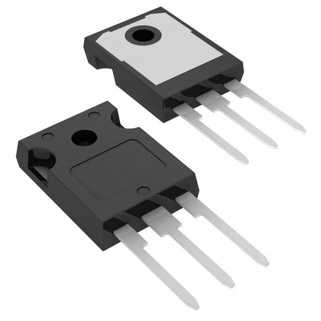
TO−247−3LD
CASE 340CH
MARKING DIAGRAM
$Y&Z&3&K
FCH
077N65F
$Y
&Z
&3
&K
FCH077N65F
= ON Semiconductor Logo
= Assembly Plant Code
= Numeric Date Code
= Lot Code
= Specific Device Code
ORDERING INFORMATION
See detailed ordering and shipping information on page 2 of
this data sheet.
© Semiconductor Components Industries, LLC, 2014
October, 2020 − Rev. 4
1
Publication Order Number:
FCH077N65F/D
�FCH077N65F
ABSOLUTE MAXIMUM RATINGS (TC = 25°C unless otherwise noted)
Symbol
Parameter
VDSS
Drain to Source Voltage
VGSS
Gate to Source Voltage
Drain Current
IDM
Drain Current
EAS
Single Pulsed Avalanche Energy (Note 2)
IAR
Avalanche Current (Note 1)
EAR
dv/dt
PD
TJ, TSTG
TL
Unit
650
V
±20
V
−DC
−AC
ID
FCH077N65F−F155
(f > 1 Hz)
±30
−Continuous (TC = 25°C)
54
−Continuous (TC = 100°C)
32
−Pulsed (Note 1)
A
162
A
1128
mJ
11
A
Repetitive Avalanche Energy (Note 1)
4.81
mJ
MOSFET dv/dt
100
V/ns
Peak Diode Recovery dv/dt (Note 3)
50
Power Dissipation
(TC = 25°C)
481
W
−Derate Above 25°C
3.85
W/°C
−55 to + 150
°C
300
°C
Operating and Storage Temperature Range
Maximum Lead Temperature for Soldering, ⅛ from Case for 5 Seconds
Stresses exceeding those listed in the Maximum Ratings table may damage the device. If any of these limits are exceeded, device functionality
should not be assumed, damage may occur and reliability may be affected.
1. Repetitive Rating: Pulse width limited by maximum junction temperature.
2. IAS = 11 A, RG = 25 W, Starting TJ = 25°C
3. ISD ≤ 27 A, di/dt ≤ 200 A/ms, VDD ≤ 380 V, Starting TJ = 25 °C.
THERMAL CHARACTERISTICS
Symbol
Parameter
RqJC
Thermal Resistance, Junction to Case, Max.
RqJA
Thermal Resistance, Junction to Ambient, Max.
符号
FCH077N65F−F155
Unit
0.26
°C/W
40
参数
FCH077N65F−F155
单位
°C/W
RqJC
结至外壳热阻最大值
0.26
RqJA
结至环境热阻最大值
40
PACKAGE MARKING AND ORDERING INFORMATION
Part Number
Top Mark
Package
Packing Method
Reel Size
Tape Width
Quantity
FCH077N65F−F155
FCH077N65F
TO−247−3LD
Tube
N/A
N/A
30 Units
www.onsemi.com
2
�FCH077N65F
ELECTRICAL CHARACTERISTICS (TC = 25°C unless otherwise noted)
Symbol
Parameter
Test Condition
Min.
Typ.
Max.
Unit
VGS = 0 V, ID = 10 mA, TJ = 25°C
650
−
−
V
VGS = 0 V, ID = 10 mA, TJ = 150°C
700
−
−
0.72
−
V/°C
mA
OFF CHARACTERISTICS
BVDSS
Drain to Source Breakdown Voltage
DBVDSS/
DTJ
Breakdown Voltage Temperature
Coefficient
ID = 10 mA, Referenced to 25°C
−
IDSS
Zero Gate Voltage Drain Current
VDS = 650 V, VGS = 0 V
−
−
10
VDS = 520 V, VGS = 0 V, TC = 125°C
−
144
−
VGS = ±20 V, VDS = 0 V
−
−
±100
nA
IGSS
Gate to Body Leakage Current
ON CHARACTERISTICS
VGS(th)
Gate Threshold Voltage
VGS = VDS, ID = 5.4 mA
3
−
5
V
RDS(on)
Static Drain to Source On Resistance
VGS = 10 V, ID = 27 A
−
68
77
mW
Forward Transconductance
VDS = 20 V, ID = 27 A
−
42
−
S
VDS = 100 V, VGS = 0 V,
f = 1 MHz
−
5345
7109
pF
−
165
220
pF
−
0.8
−
pF
−
pF
gFS
DYNAMIC CHARACTERISTICS
Ciss
Input Capacitance
Coss
Output Capacitance
Crss
Reverse Transfer Capacitance
Coss
Output Capacitance
VDS = 380 V, VGS = 0 V, f = 1 MHz
−
97
Effective Output Capacitance
VDS = 0 V to 400 V, VGS = 0 V
−
693
−
pF
Total Gate Charge at 10 V
VDD = 380 V, ID = 27 A,
VGS = 10 V
(Note 4)
−
126
164
nC
−
28
−
nC
−
53
−
nC
f = 1 MHz
−
0.7
−
W
VDD = 380 V, ID = 27 A,
VGS = 10 V, RG = 4.7 W
(Note 4)
−
40
90
ns
−
35
80
ns
Coss(eff.)
Qg(tot)
Qgs
Gate to Source Gate Charge
Qgd
Gate to Drain “Miller”Charge
ESR
Equivalent Series Resistance
SWITCHING CHARACTERISTICS
td(on)
Turn-On Delay Time
tr
Turn-On Rise Time
td(off)
Turn-Off Delay Time
−
113
236
ns
Turn-Off Fall Time
−
5
20
ns
Maximum Continuous Drain to Source Diode Forward Current
−
−
54
A
ISM
Maximum Pulsed Drain to Source Diode Forward Current
−
−
162
A
VSD
tf
DRAIN-SOURCE DIODE CHARACTERISTICS
IS
Drain to Source Diode Forward Voltage
VGS = 0 V, ISD = 27 A
−
−
1.2
V
trr
Reverse Recovery Time
−
163
−
ns
Qrr
Reverse Recovery Charge
VGS = 0 V, ISD = 27 A,
dIF/dt = 100 A/ms
−
0.9
−
mC
Product parametric performance is indicated in the Electrical Characteristics for the listed test conditions, unless otherwise noted. Product
performance may not be indicated by the Electrical Characteristics if operated under different conditions.
4. Essentially independent of operating temperature.
www.onsemi.com
3
�FCH077N65F
TYPICAL PERFORMANCE CHARACTERISTICS
200
VGS = 10.0 V
8.0 V
7.0 V
6.5 V
6.0 V
5.5 V
100
10
1
*Notes:
1. VDS = 20 V
2. 250 ms Pulse Test
100
ID, Drain Current (A)
ID, Drain Current (A)
1000
150°C
10
−55°C
*Notes:
1. 250 ms Pulse Test
2. TC = 25°C
0.1
10
1
25°C
1
20
3
VDS, Drain−Source Voltage (V)
IS, Reverse Drain Current (A)
RDS(ON), Drain−Source On−Resistance (W)
1000
*Note: TC = 25°C
0.10
VGS = 10 V
0.08
VGS = 20 V
0
32
64
96
128
100
10
150°C
1
25°C
0.1
0.01
0.001
0.0
160
10
1
VGS, Gate−Source Voltage (V)
Capacitance (pF)
10000
Ciss
10
Coss
Ciss = Cgs + Cgd (Cds = Shorted)
Coss = Cds + Cgd
Crss = Cgd
0.1
0.1
1
10
0.8
1.2
1.6
2.0
Figure 4. Body Diode Forward Voltage Variation
vs. Source Current and Temperature
100000
*Note:
1. VGS = 0 V
2. f = 1 MHz
0.4
VSD, Body Diode Forward Voltage (V)
Figure 3. On−Resistance Variation vs. Drain
Current and Gate Voltage
100
8
*Notes:
1. VGS = 0 V
2. 250 ms Pulse Test
ID, Drain Current (A)
1000
7
Figure 2. Transfer Characteristics
0.12
0.06
6
VGS, Gate−Source Voltage (V)
Figure 1. On−Region Characteristics
0.14
5
4
Crss
100
8
VDS, Drain−Source Voltage (V)
VDS = 130 V
VDS = 325 V
6
VDS = 520 V
4
2
0
700
*Note: ID = 27 A
0
26
52
78
104
Qg, Total Gate Charge (nC)
130
Figure 6. Gate Charge Characteristics
Figure 5. Capacitance Characteristics
www.onsemi.com
4
�FCH077N65F
TYPICAL PREFORMANCE CHARACTERISTICS (continued)
2.5
*Notes:
1. VGS = 0 V
2. ID = 10 mA
1.1
RDS(on), (Normalized)
Drain−Source On−Resistance
BVDSS, (Normalized)
Drain−Source Breakdown Voltage
1.2
1.0
0.9
0.8
−100
−50
0
50
100
150
2.0
*Notes:
1. VGS = 10V
2. ID = 27A
1.5
1.0
0.5
−100
200
TJ, Junction Temperature (°C)
150
200
10 ms
ID, Drain Current (A)
ID, Drain Current (A)
100
Figure 8. On−Resistance Variation
vs. Temperature
100 ms
10
1 ms
Operation in This Area
is Limited by RDS(on)
DC
*Notes:
1. TC = 25°C
2. TJ = 150°C
3. Single Pulse
1
1
10
100
24
18
12
6
260
24
390
520
25
50
75
100
125
TC, Case Temperature (°C)
Figure 10. Maximum Drain Current
vs. Case Temperature
30
130
36
0
1000
VDS, Drain−Source Voltage (V)
0
48
12
Figure 9. Maximum Safe Operating Area
EOSS (mJ)
50
60
200
100
0
0
TJ, Junction Temperature (°C)
Figure 7. Breakdown Voltage Variation
vs. Temperature
0.1
−50
650
VDS, Drain to Source Voltage (V)
Figure 11. EOSS vs. Drain to Source Voltage
www.onsemi.com
5
150
�FCH077N65F
ZqJC(t), Thermal Response (°C/W)
TYPICAL PERFORMANCE CHARACTERISTICS (continued)
1
0.1
0.5
0.2
PDM
0.1
0.05
0.01 0.02
0.01
Single Pulse
0.001
10−5
10−4
t1
t2
*Notes:
1. ZqJC(t) = 0.26°C/W Max.
2. Duty Factor, D = t1/t2
3. TJM − TC = PDM * ZqJC(t)
10−3
10−2
10−1
t1, Rectangular Pulse Duration (sec)
Figure 12. Transient Thermal Response Curve
www.onsemi.com
6
1
�FCH077N65F
VGS
RL
Qg
VDS
VGS
Qgs
Qgd
DUT
IG = Const.
Charge
Figure 13. Transient Thermal Response Curve
RL
VDS
VDS
90%
90%
90%
VDD
VGS
RG
VGS
DUT
VGS
10%
td(on)
10%
tr
tf
td(off)
ton
toff
Figure 14. Resistive Switching Test Circuit & Waveforms
L
E AS + 1 @ LI AS
2
VDS
BVDSS
ID
IAS
RG
VDD
DUT
VGS
2
ID(t)
VDD
VDS(t)
tp
tp
Figure 15. Unclamped Inductive Switching Test Circuit & Waveforms
www.onsemi.com
7
Time
�FCH077N65F
+
DUT
VDS
−
ISD
L
Driver
RG
Same Type
as DUT
VGS
− dv/dt controlled by RG
− ISD controlled by pulse period
D+
VGS
(Driver)
VDD
Gate Pulse Width
Gate Pulse Period
10 V
IFM, Body Diode Forward Current
ISD
(DUT)
di/dt
IRM
Body Diode Reverse Current
Body Diode Recovery dv/dt
VDS
(DUT)
VDD
VSD
Body Diode
Forward Voltage Drop
Figure 16. Peak Diode Recovery dv/dt Test Circuit & Waveforms
SUPERFET is a registered trademark of Semiconductor Components Industries, LLC (SCILLC) or its subsidiaries in the United States and/or
other countries.
FRFET is a registered trademark of Semiconductor Components Industries, LLC (SCILLC) or its subsidiaries in the United States and/or other
countries.
www.onsemi.com
8
�MECHANICAL CASE OUTLINE
PACKAGE DIMENSIONS
TO−247−3LD
CASE 340CH
ISSUE A
DATE 09 OCT 2019
GENERIC
MARKING DIAGRAM*
XXXXXXXXX
AYWWG
XXXX
A
Y
WW
G
= Specific Device Code
= Assembly Location
= Year
= Work Week
= Pb−Free Package
*This information is generic. Please refer to
device data sheet for actual part marking.
Pb−Free indicator, “G” or microdot “G”, may
or may not be present. Some products may
not follow the Generic Marking.
DOCUMENT NUMBER:
DESCRIPTION:
98AON13853G
TO−247−3LD
Electronic versions are uncontrolled except when accessed directly from the Document Repository.
Printed versions are uncontrolled except when stamped “CONTROLLED COPY” in red.
PAGE 1 OF 1
ON Semiconductor and
are trademarks of Semiconductor Components Industries, LLC dba ON Semiconductor or its subsidiaries in the United States and/or other countries.
ON Semiconductor reserves the right to make changes without further notice to any products herein. ON Semiconductor makes no warranty, representation or guarantee regarding
the suitability of its products for any particular purpose, nor does ON Semiconductor assume any liability arising out of the application or use of any product or circuit, and specifically
disclaims any and all liability, including without limitation special, consequential or incidental damages. ON Semiconductor does not convey any license under its patent rights nor the
rights of others.
© Semiconductor Components Industries, LLC, 2018
www.onsemi.com
�onsemi,
, and other names, marks, and brands are registered and/or common law trademarks of Semiconductor Components Industries, LLC dba “onsemi” or its affiliates
and/or subsidiaries in the United States and/or other countries. onsemi owns the rights to a number of patents, trademarks, copyrights, trade secrets, and other intellectual property.
A listing of onsemi’s product/patent coverage may be accessed at www.onsemi.com/site/pdf/Patent−Marking.pdf. onsemi reserves the right to make changes at any time to any
products or information herein, without notice. The information herein is provided “as−is” and onsemi makes no warranty, representation or guarantee regarding the accuracy of the
information, product features, availability, functionality, or suitability of its products for any particular purpose, nor does onsemi assume any liability arising out of the application or use
of any product or circuit, and specifically disclaims any and all liability, including without limitation special, consequential or incidental damages. Buyer is responsible for its products
and applications using onsemi products, including compliance with all laws, regulations and safety requirements or standards, regardless of any support or applications information
provided by onsemi. “Typical” parameters which may be provided in onsemi data sheets and/or specifications can and do vary in different applications and actual performance may
vary over time. All operating parameters, including “Typicals” must be validated for each customer application by customer’s technical experts. onsemi does not convey any license
under any of its intellectual property rights nor the rights of others. onsemi products are not designed, intended, or authorized for use as a critical component in life support systems
or any FDA Class 3 medical devices or medical devices with a same or similar classification in a foreign jurisdiction or any devices intended for implantation in the human body. Should
Buyer purchase or use onsemi products for any such unintended or unauthorized application, Buyer shall indemnify and hold onsemi and its officers, employees, subsidiaries, affiliates,
and distributors harmless against all claims, costs, damages, and expenses, and reasonable attorney fees arising out of, directly or indirectly, any claim of personal injury or death
associated with such unintended or unauthorized use, even if such claim alleges that onsemi was negligent regarding the design or manufacture of the part. onsemi is an Equal
Opportunity/Affirmative Action Employer. This literature is subject to all applicable copyright laws and is not for resale in any manner.
PUBLICATION ORDERING INFORMATION
LITERATURE FULFILLMENT:
Email Requests to: orderlit@onsemi.com
onsemi Website: www.onsemi.com
◊
TECHNICAL SUPPORT
North American Technical Support:
Voice Mail: 1 800−282−9855 Toll Free USA/Canada
Phone: 011 421 33 790 2910
Europe, Middle East and Africa Technical Support:
Phone: 00421 33 790 2910
For additional information, please contact your local Sales Representative
�