FCPF360N65S3R0L
MOSFET – Power, N-Channel,
SUPERFET III, Easy Drive
650 V, 10 A, 360 mW
Description
SUPERFET III MOSFET is ON Semiconductor’s brand−new high
voltage super−junction (SJ) MOSFET family that is utilizing charge
balance technology for outstanding low on−resistance and lower gate
charge performance. This advanced technology is tailored to minimize
conduction loss, provides superior switching performance, and
withstand extreme dv/dt rate. Consequently, SUPERFET III MOSFET
Easy drive series helps manage EMI issues and allows for easier
design implementation.
www.onsemi.com
VDSS
RDS(ON) MAX
ID MAX
650 V
360 mW @ 10 V
10 A
D
Features
•
•
•
•
•
•
700 V @ TJ = 150°C
Typ. RDS(on) = 310 mW
Ultra Low Gate Charge (Typ. Qg = 18 nC)
Low Effective Output Capacitance (Typ. Coss(eff.) = 173 pF)
100% Avalanche Tested
These Devices are Pb−Free and are RoHS Compliant
G
S
N-Channel MOSFET
Applications
•
•
•
•
Computing / Display Power Supplies
Telecom / Server Power Supplies
Industrial Power Supplies
Lighting / Charger / Adapter
G
D
S
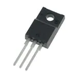
TO−220F
CASE 340BF
MARKING DIAGRAM
$Y&Z&3&K
FCPF360
N65S3R0
$Y
&Z
&3
&K
FCPF360N65S3R0
= ON Semiconductor Logo
= Assembly Plant Code
= Data Code (Year & Week)
= Lot
= Specific Device Code
ORDERING INFORMATION
See detailed ordering and shipping information on page 2 of
this data sheet.
© Semiconductor Components Industries, LLC, 2017
August, 2019 − Rev. 3
1
Publication Order Number:
FCPF360N65S3R0L/D
�FCPF360N65S3R0L
ABSOLUTE MAXIMUM RATINGS (TC = 25°C, Unless otherwise specified)
Symbol
Parameter
VDSS
Drain to Source Voltage
VGSS
Gate to Source Voltage
ID
Drain Current
Value
Unit
650
V
DC
±30
V
AC (f > 1 Hz)
±30
V
Continuous (TC = 25°C)
10*
A
Continuous (TC = 100°C)
6*
Pulsed (Note 1)
IDM
Drain Current
25*
A
EAS
Single Pulsed Avalanche Energy (Note 2)
40
mJ
IAS
Avalanche Current (Note 2)
2.1
A
EAR
Repetitive Avalanche Energy (Note 1)
0.27
mJ
dv/dt
MOSFET dv/dt
100
V/ns
Peak Diode Recovery dv/dt (Note 3)
20
PD
Power Dissipation
(TC = 25°C)
27
W
0.22
W/°C
−55 to +150
°C
300
°C
Derate Above 25°C
TJ, TSTG
TL
Operating and Storage Temperature Range
Maximum Lead Temperature for Soldering, 1/8″ from Case for 5 s
Stresses exceeding those listed in the Maximum Ratings table may damage the device. If any of these limits are exceeded, device functionality
should not be assumed, damage may occur and reliability may be affected.
*Drain current limited by maximum junction temperature.
1. Repetitive rating: pulse-width limited by maximum junction temperature.
2. IAS = 2.1 A, RG = 25 W, starting TJ = 25°C.
3. ISD ≤ 5 A, di/dt ≤ 200 A/ms, VDD ≤ 400 V, starting TJ = 25°C.
THERMAL CHARACTERISTICS
Symbol
Parameter
Value
Unit
_C/W
RqJC
Thermal Resistance, Junction to Case, Max.
4.56
RqJA
Thermal Resistance, Junction to Ambient, Max.
62.5
PACKAGE MARKING AND ORDERING INFORMATION
Part Number
Top Marking
Package
Packing Method
Reel Size
Tape Width
Quantity
FCPF360N65S3R0L
FCPF360N65S3R0
TO−220F
Tube
N/A
N/A
50 Units
www.onsemi.com
2
�FCPF360N65S3R0L
ELECTRICAL CHARACTERISTICS (TC = 25°C unless otherwise noted)
Parameter
Symbol
Test Conditions
Min
Typ
Max
Unit
VGS = 0 V, ID = 1 mA, TJ = 25_C
650
−
−
V
VGS = 0 V, ID = 1 mA, TJ = 150_C
700
−
−
V
OFF CHARACTERISTICS
BVDSS
Drain to Source Breakdown Voltage
DBVDSS/DTJ
Breakdown Voltage Temperature
Coefficient
ID = 1 mA, Referenced to 25_C
−
0.68
−
V/_C
IDSS
Zero Gate Voltage Drain Current
VDS = 650 V, VGS = 0 V
−
−
1
mA
VDS = 520 V, TC = 125_C
−
0.58
−
IGSS
Gate to Body Leakage Current
VGS = ±30 V, VDS = 0 V
−
−
±100
nA
2.5
−
4.5
V
ON CHARACTERISTICS
VGS(th)
Gate Threshold Voltage
VGS = VDS, ID = 0.2 mA
RDS(on)
Static Drain to Source On Resistance
VGS = 10 V, ID = 5 A
−
310
360
mW
Forward Transconductance
VDS = 20 V, ID = 5 A
−
6
−
S
VDS = 400 V, VGS = 0 V, f = 1 MHz
−
730
−
pF
−
15
−
pF
gFS
DYNAMIC CHARACTERISTICS
Ciss
Input Capacitance
Coss
Output Capacitance
Coss(eff.)
Effective Output Capacitance
VDS = 0 V to 400 V, VGS = 0 V
−
173
−
pF
Coss(er.)
Energy Related Output Capacitance
VDS = 0 V to 400 V, VGS = 0 V
−
26
−
pF
Total Gate Charge at 10 V
VDS = 400 V, ID = 5 A, VGS = 10 V
(Note 4)
−
18
−
nC
−
4.3
−
nC
Qg(tot)
Qgs
Gate to Source Gate Charge
Qgd
Gate to Drain “Miller” Charge
ESR
Equivalent Series Resistance
−
7.6
−
nC
f = 1 MHz
−
1
−
W
VDD = 400 V, ID = 5 A,
VGS = 10 V, Rg = 4.7 W
(Note 4)
−
12
−
ns
−
11
−
ns
SWITCHING CHARACTERISTICS
td(on)
Turn-On Delay Time
tr
Turn-On Rise Time
td(off)
Turn-Off Delay Time
−
34
−
ns
Turn-Off Fall Time
−
10
−
ns
Maximum Continuous Source to Drain Diode Forward Current
−
−
10
A
ISM
Maximum Pulsed Source to Drain Diode Forward Current
−
−
25
A
VSD
Source to Drain Diode Forward
Voltage
VGS = 0 V, ISD = 5 A
−
−
1.2
V
trr
Reverse Recovery Time
−
241
−
ns
Qrr
Reverse Recovery Charge
VGS = 0 V, ISD = 5 A,
dIF/dt = 100 A/ms
−
2.4
−
mC
tf
SOURCE-DRAIN DIODE CHARACTERISTICS
IS
Product parametric performance is indicated in the Electrical Characteristics for the listed test conditions, unless otherwise noted. Product
performance may not be indicated by the Electrical Characteristics if operated under different conditions.
4. Essentially independent of operating temperature typical characteristics.
www.onsemi.com
3
�FCPF360N65S3R0L
TYPICAL PERFORMANCE CHARACTERISTICS
ID, Drain Current[A]
10
50
VGS = 10.0V
8.0V
7.0V
6.5V
6.0V
5.5V
ID, Drain Current[A]
50
1
*Notes:
1. VDS = 20V
2. 250 ms Pulse Test
10
o
150 C
o
25 C
1
o
−55 C
*Notes:
1. 250 ms Pulse Test
o
2. TC = 25 C
0.1
0.2
1
10
VDS, Drain−Source Voltage[V]
0.1
20
2
Figure 1. On-Region Characteristics
*Notes:
1. VGS = 0V
1.0
0.8
0.6
VGS = 10V
VGS = 20V
0.2
0.0
0
5
10
15
20
ID, Drain Current [A]
25
10
o
1
o
25 C
0.1
o
VGS, Gate−Source Voltage [V]
Capacitances [pF]
10000
1
Ciss
Coss
*Note:
1. VGS = 0V
2. f = 1MHz
Ciss = C gs + Cgd (C ds = shorted)
Coss = C ds + Cgd
Crss = Cgd
0.1
0.1
1
10
100
VDS, Drain−Source Voltage [V]
0.0
0.5
1.0
VSD, Body Diode Forward Voltage [V]
1.5
Figure 4. Body Diode Forward Voltage
Variation vs. Source Current and Temperature
10
100
−55 C
0.01
100000
1000
2. 250 ms Pulse Test
150 C
0.001
30
Figure 3. On-Resistance Variation vs. Drain
Current and Gate Voltage
10
8
100
o
*Note: TC = 25 C
0.4
4
5
6
7
VGS, Gate−Source Voltage[V]
Figure 2. Transfer Characteristics
IS, Reverse Drain Current [A]
RDS(ON),
Drain−Source On−Resistance [W ]
1.2
3
Crss
8
Figure 5. Capacitance Characteristics
VDS = 130V
VDS = 400V
6
4
2
0
1000
*Note: I D = 5A
0
5
10
15
Qg, Total Gate Charge [nC]
Figure 6. Gate Charge Characteristics
www.onsemi.com
4
20
�FCPF360N65S3R0L
TYPICAL PERFORMANCE CHARACTERISTICS (Continued)
3.0
*Notes:
1. VGS = 0V
2. I D = 10mA
1.1
RDS(on), [Normalized]
Drain−Source On−Resistance
BVDSS, [Normalized]
Drain−Source Breakdown Voltage
1.2
1.0
0.9
0.8
−50
0
50
100
o
TJ, Junction Temperature [ C]
1.0
0.5
−50
0
50
100
o
TJ, Junction Temperature [ C]
150
12
10
30m s
10
ID, Drain Current [A]
100m s
1ms
10ms
1
Operation in This Area
is Limited by R DS(on)
DC
*Notes:
0.1
o
1. TC = 25 C
2. TJ = 150 C
3. Single Pulse
1
10
100
VDS, Drain−Source Voltage [V]
4
3
2
1
130
260
390
520
VDS, Drain to Source Voltage [V]
4
25
50
75
100
125
TC, Case Temperature [ o C]
150
Figure 10. Maximum Drain Current
vs. Case Temperature
5
0
6
0
1000
Figure 9. Maximum Safe Operation Area
0
8
2
o
EOSS [m J]
1.5
Figure 8. On-Resistance Variant vs. Temperature
100
ID, Drain Current [A]
2.0
0.0
150
Figure 7. Breakdown Voltage Variation
vs. Temperature
0.01
2.5
*Notes:
1. VGS = 10V
2. I D = 5A
650
Figure 11. EOSS vs. Drain to Source Voltage
www.onsemi.com
5
�FCPF360N65S3R0L
r(t), NORMALIZED EFFECTIVE TRANSIENT
THERMAL RESISTANCE
TYPICAL PERFORMANCE CHARACTERISTICS (Continued)
2
1
0.1
DUTY CYCLE−DESCENDING ORDER
D = 0.5
0.2
0.1
0.05
0.02
0.01
PDM
t1
t2
0.01
0.001
−5
10
NOTES:
Z qJC(t) = r(t) x RqJC
RqJC = 4.56 oC/W
Peak T J = PDM x ZqJC(t) + TC
Duty Cycle, D = t1 / t2
SINGLE PULSE
−4
10
−3
10
−2
−1
10
10
t, RECTANGULAR PULSE DURATION (sec)
Figure 12. Transient Thermal Response Curve
www.onsemi.com
6
0
10
1
10
2
10
�FCPF360N65S3R0L
Figure 13. Gate Charge Test Circuit & Waveform
VDS
RG
V
10V
GS
RL
VDS
90%
VDD
VGS
VGS
DUT
10%
tr
td(on)
t on
Figure 14. Resistive Switching Test Circuit & Waveforms
Figure 15. Unclamped Inductive Switching Test Circuit & Waveforms
www.onsemi.com
7
td(off)
t off
tf
�FCPF360N65S3R0L
+
DUT
VDS
_
I SD
L
Driver
RG
Same Type
as DUT
VGS
VGS
( Driver )
I SD
( DUT )
VDD
Sdv/dt controlled by R G
SI SD controlled by pulse period
D=
Gate Pulse Width
Gate Pulse Period
10V
IFM , Body Diode Forward Current
di/dt
IRM
Body Diode Reverse Current
VDS
( DUT )
Body Diode Recoverydv/dt
VSD
VDD
Body Diode
Forward Voltage Drop
Figure 16. Peak Diode Recovery dv/dt Test Circuit & Waveforms
SUPERFET is a registered trademark of Semiconductor Components Industries, LLC (SCILLC) or its subsidiaries in the United States and/or
other countries.
www.onsemi.com
8
�MECHANICAL CASE OUTLINE
PACKAGE DIMENSIONS
TO−220 FULLPAK 3LD
CASE 340BF
ISSUE O
DATE 31 AUG 2016
10.30
9.80
A
2.90
2.50
3.40
3.00
3.00
2.60
B 19.00
17.70
6.60
6.20
1 X 45°
B 15.70
15.00
3.30 B
2.70
3
1
2.14
10.70
10.30
NOTES:
2.74 (2X)
2.34
4.60
4.30
DESCRIPTION:
B 0.60
0.40
0.90 (3X)
0.50
0.50 M A
1.20
1.00
DOCUMENT NUMBER:
2.70
2.30
1.20(2X)
0.90
98AON13839G
TO−220 FULLPAK 3LD
A. EXCEPT WHERE NOTED CONFORMS TO
EIAJ SC91A.
B DOES NOT COMPLY EIAJ STD. VALUE.
C. ALL DIMENSIONS ARE IN MILLIMETERS.
D. DIMENSIONS ARE EXCLUSIVE OF BURRS,
MOLD FLASH AND TIE BAR PROTRUSIONS.
E. DIMENSION AND TOLERANCE AS PER ASME
Y14.5−2009.
Electronic versions are uncontrolled except when accessed directly from the Document Repository.
Printed versions are uncontrolled except when stamped “CONTROLLED COPY” in red.
PAGE 1 OF 1
ON Semiconductor and
are trademarks of Semiconductor Components Industries, LLC dba ON Semiconductor or its subsidiaries in the United States and/or other countries.
ON Semiconductor reserves the right to make changes without further notice to any products herein. ON Semiconductor makes no warranty, representation or guarantee regarding
the suitability of its products for any particular purpose, nor does ON Semiconductor assume any liability arising out of the application or use of any product or circuit, and specifically
disclaims any and all liability, including without limitation special, consequential or incidental damages. ON Semiconductor does not convey any license under its patent rights nor the
rights of others.
© Semiconductor Components Industries, LLC, 2019
www.onsemi.com
�onsemi,
, and other names, marks, and brands are registered and/or common law trademarks of Semiconductor Components Industries, LLC dba “onsemi” or its affiliates
and/or subsidiaries in the United States and/or other countries. onsemi owns the rights to a number of patents, trademarks, copyrights, trade secrets, and other intellectual property.
A listing of onsemi’s product/patent coverage may be accessed at www.onsemi.com/site/pdf/Patent−Marking.pdf. onsemi reserves the right to make changes at any time to any
products or information herein, without notice. The information herein is provided “as−is” and onsemi makes no warranty, representation or guarantee regarding the accuracy of the
information, product features, availability, functionality, or suitability of its products for any particular purpose, nor does onsemi assume any liability arising out of the application or use
of any product or circuit, and specifically disclaims any and all liability, including without limitation special, consequential or incidental damages. Buyer is responsible for its products
and applications using onsemi products, including compliance with all laws, regulations and safety requirements or standards, regardless of any support or applications information
provided by onsemi. “Typical” parameters which may be provided in onsemi data sheets and/or specifications can and do vary in different applications and actual performance may
vary over time. All operating parameters, including “Typicals” must be validated for each customer application by customer’s technical experts. onsemi does not convey any license
under any of its intellectual property rights nor the rights of others. onsemi products are not designed, intended, or authorized for use as a critical component in life support systems
or any FDA Class 3 medical devices or medical devices with a same or similar classification in a foreign jurisdiction or any devices intended for implantation in the human body. Should
Buyer purchase or use onsemi products for any such unintended or unauthorized application, Buyer shall indemnify and hold onsemi and its officers, employees, subsidiaries, affiliates,
and distributors harmless against all claims, costs, damages, and expenses, and reasonable attorney fees arising out of, directly or indirectly, any claim of personal injury or death
associated with such unintended or unauthorized use, even if such claim alleges that onsemi was negligent regarding the design or manufacture of the part. onsemi is an Equal
Opportunity/Affirmative Action Employer. This literature is subject to all applicable copyright laws and is not for resale in any manner.
PUBLICATION ORDERING INFORMATION
LITERATURE FULFILLMENT:
Email Requests to: orderlit@onsemi.com
onsemi Website: www.onsemi.com
◊
TECHNICAL SUPPORT
North American Technical Support:
Voice Mail: 1 800−282−9855 Toll Free USA/Canada
Phone: 011 421 33 790 2910
Europe, Middle East and Africa Technical Support:
Phone: 00421 33 790 2910
For additional information, please contact your local Sales Representative
�