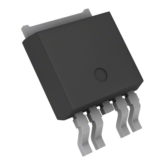
FDDS100H06_F085
Smart High Side Switch
Features
Description
• Short circuit protection
N channel power FET with charge pump, ground referenced
CMOS compatible input and diagnostic output with integrated
protective functions.
• Current limitation
• Thermal shutdown with restart.
TO252-5L
• Overvoltage protection(including load dump)
• Very low standby current
3
• Under voltage and over voltage shutdown with auto-restart
and hysteresis.
1
• Fast demagnetization of inductive loads
5
• Open load detection in ON-state
• CMOS compatible input
• ESD protection
• Optimized static electromagnetic compatibility
• Open drain fault output
• Qualified to AEC Q100
Typical Applications
• Power switch with diagnostic feedback for DC ground loads
• All types of resistive, inductive, and capacitive loads
Ordering Information
• Replace electromechanical relays, fuses and discrete circuits
Device
Package
FDDS100H06_F085 TO252- 5L
©2011 Fairchild Semiconductor Corporation
FDDS100H06_F085 Rev. 1.0.0
1
Operating
Temp.
-40 C ~ 150 C
www.fairchildsemi.com
FDDS100H06_F085 Smart High Side Switch
September 2011
�VBB
Charge
Pump
Voltage
Source
Battery
Voltage
Sensor
IN
4
SenseFET
LoadCurrent
Limiter
LoadCurrent
Sensor
OUT
5
Temperature
Sensor
ESD
&
Overvoltage
Protection
ST
Output
Clamp&Gate
Protection
Gate Driver
Undervoltage
&
Overvoltage
2
3
Control Logic
Output
Voltage
Detection
GND
1
Pin Definitions
Pin Number
Pin Name
I/O
Pin Function Description
1
GND
P
Ground
2
IN
A
Input, activates the power switch in case of logic high
3
Vbb
P
Supply voltage; Pin3 and TAB are internally shorted
4
ST
A
Fault signal feedback; low on failure
5
OUT
A
Output to loads
©2011 Fairchild Semiconductor Corporation
FDDS100H06_F085 Rev. 1.0.0
2
www.fairchildsemi.com
FDDS100H06_F085 Smart High Side Switch
Block Diagrams
�At Tj=25C unless otherwise specified.
Parameter
Supply voltage
1)
Supply voltage for full short circuit protection
Load dump protection VLoadDump = UA + VS, UA=13.5V
RI=2, RL=12, td=400ms, IN=Low o r High
Load current (Short-circuit current) 3)
Symbol
Values
Unit
Vbb
37
V
Vbb
34
V
VLoadDump 2)
60
V
IL
Self-limited
V
Tj
Tstg
-40 ~ 150
-55 ~ 150
C
C
Ptot
41.6
W
Inductive load switch-off energy dissipation
Single pulse, IL= 2.67A, L=100mH, Vbb=12V, Tj=150C
EAS
0.425
J
Electrostatic discharge capability
(ESD)
VESD
4
KV
2
KV
Operating temperature range
Storage temperature range
Power Dissipation(DC) TC ≤25 °C
4)
HBM (Human Body Model)
CDM (Charged Device Model)
Input Voltage (DC)
VIN
-0.5 .... + 5.4
V
Current through input pin(DC)
Current through status pin(DC)
IIN
IST
+/-2
+/-5
mA
Note:
1) See also on page 04.
2) VLoad dump is setup without the DUT connected to the generator.
3) See also diagram on page 05.
4) not subject to production test, specified by design. See also on page 10.
©2011 Fairchild Semiconductor Corporation
FDDS100H06_F085 Rev. 1.0.0
3
www.fairchildsemi.com
FDDS100H06_F085 Smart High Side Switch
Absolute Maximum Ratings
�At Tj=25C, Vbb=12V unless otherwise specified.
Parameter
Symbol
Conditions
RthJC
RthJA
(junction to case)
Mini. footprint (junction to ambient)
1 Inch^2 device on PCB 1)
Min. Typ. Max. Unit
Theramal Characteristics
Thermal resistance
-
99
35
45
3
K/W
Load Switching Capability and Characteristics
On-state resistance(Pin3 to pin 5)
RON
VIN=5V, Vbb=12V, IL=2.5A Tj=25C
VIN=5V, Vbb=12V, IL=2.5A Tj=150C
-
80
160
100
200
m
Nominal load current( tab to pin5)
IL(NOM)
SMD1) VON 5.5V
©2011 Fairchild Semiconductor Corporation
FDDS100H06_F085 Rev. 1.0.0
4
www.fairchildsemi.com
FDDS100H06_F085 Smart High Side Switch
Electrical Characteristics
�At Tj=25C, Vbb=12V unless otherwise specified
Parameter
Protection Functions
Symbol
Conditions
Min. Typ. Max. Unit
IL(SCP)
Tj=-40C
Tj=25C
Tj=150C
9
7
4
-
4
-
V
td(SC)
Tj=-40C ~ 150C
Minimum Input low time : 60us
80
250
530
us
VON(CL)
IL=40mA
Tj=-40C ~ 150C
50
56.5
63
V
150
170
-
C
-
10
-
K
-
-
32
V
-
480
mA
1)
Short circuit current limit (pin3 to pin 5)
VON > VON(SC)
Short Circuit detection voltage
Short Circuit shutdown delay time
Output clamp(inductive load switch off)
at VOUT= Vbb-VON(CL)(overvoltage) 2)
Thermal overload trip temperature
VON(SC)
Tjt
Thermal hysteresis
Tjt
Reverse battery voltage 3)
-Vbb
VIN =5V
15
12
7
24
19
10
A
Diagnostic Characteristics
Open load detection current
IL(OL)
VIN =5V,Tj=-40 ~ 150C
12
RI
Tj=-40 ~ 150C
2.4
3.0
3.6
K
VINH
Tj=-40 ~ 150C
-
2.2
2.9
V
Input & Status Feedback 4)
Input Resistance
Input turn-on threshold voltage
Input turn-off threshold voltage
VINL
Tj=-40 ~ 150C
1.2
-
-
V
Off state input current
IIN(OFF)
VIN=0V, Tj=-40 ~ 150C
-
-
1
uA
On state input current
IIN(ON)
VIN=3.5V, Tj=-40 ~ 150C
20
45
70
uA
Initial open load delay time
td(ST)
Tj=-40 ~ 150C
-
380
750
us
Delay time for status with open load
while ON 5)
td(ON_OL)
Normal --> Open load, Tj=-40 ~ 150C
10
30
90
us
Delay time for status with open load
while ON
td(ON_Nor)
Open load --> Normal, Tj=-40 ~ 150C
10
30
90
us
Status output(open drain) for high level
VSTH
IST=1.6mA, Tj=-40 ~ 150C
5.4
6.3
Status output(open drain) for low level
VSTL
IST=1.6mA, Tj=-40 ~ 150C
-
V
0.6
V
notes:
1) Integrated protection functions are designed to prevent IC destruction under fault conditions described in the data sheet. Fault conditions are considered as "outside" normal
operating range. Protection functions are not designed for continuous repetitive operation.
2) See the page12
3) Requoired 150 resistor in GND PIN. Note that the power dissipation is higher compared to normal operation condition due to the voltage drop across the intrinsic drainsource diode. The temperature protection is not active during reversrse current operation. IN and ST currents have to be limitted by max rating.
4) If a ground resistor RGND is used, add the voltage drop across this resistor.
5) Guaranteed by design.
©2011 Fairchild Semiconductor Corporation
FDDS100H06_F085 Rev. 1.0.0
5
www.fairchildsemi.com
FDDS100H06_F085 Smart High Side Switch
Electrical Characteristics
�FDDS100H06_F085 Smart High Side Switch
Application Information
1. Truth Table
Sense current under fault conditions
Output Level
Status
Normal operation
Input Level
L
H
L
H
H
H
Open load
L
H
X1)
H
H
L
Short circuit to Vbb
L
H
H
H
L 2)
H (L 3) )
Short circuit to GND
L
H
L
L
H
L 4)
Overtemperature
L
H
L
L
L
Undervoltage
L
H
L
L
H
H (L 5) )
Overvoltage shutdown
L
H
L
L
H
H
L
L = “ LOW “ Level, Z = High impedance, potential depends on external circuit, H = “HIGH” Level
Notes:
1) Power TR off, high impedance.
2) An short of output to Vbb ,in the off state, causes an internal current from output to ground. If RGND is used, an offset voltage at the GND and ST pins will occure and VSTL
signal may be errorious.
3) Low resistance to Vbb may be detected in ON-state by the no-load-detection.
4) Latched and reset by input. Low resistance to Vbb may be detected in ON-state by the no-load-detection.
5) Should reset IN to restart in case battery voltage comes back to normal operating range after undervoltage shutdown and status = “Low” level.
2.Terms
Ibb
IN
VIN
Vbb
IST
VON
IIN
V bb
OUT
ST
IL
GND
VOUT
VST
IGND
R GND
Notes:
©2011 Fairchild Semiconductor Corporation
FDDS100H06_F085 Rev. 1.0.0
6
www.fairchildsemi.com
�FDDS100H06_F085 Smart High Side Switch
3. Detailed Function Blocks
3.1 Input circuit (ESD protection)
RI
IN
VZI1
VZI2
GND
VZI1 = 16V (typ.), VZI2 = 6.1V (typ.). RI=3K.
3.2 Status output
5V
IS T
ST
D Z ,S T
GND
VDZ,ST = 6.1V (typ.), Max 5mA. with IST =1.6mA. Low level of ST is 0.6(Max).
3.3 Inductive and overvoltage output clamp
Vbb
VZ1
VON
OUT
VON is clamped to VON(CL)=59V(Typ).
3.4 Overvoltage and reverse battery protection
VBB
VBB
R IN
RI
IN
ST
R ST
D Z,ST
R IN
Logic
RI
Logic
ST
V bb(AZ)
V ZI1
IN
R ST
V ZI2
D Z,ST
V bb(AZ)
V ZI1
V ZI2
GND
GND
R GND
Schottky
Diode
VDZ,ST =6.1V(Typ), VZI1 = 16V (typ.), VZI2 = 6.1V(Typ). RGND = 150 typ.Vbb(AZ) = 54V(typ).
©2011 Fairchild Semiconductor Corporation
FDDS100H06_F085 Rev. 1.0.0
7
www.fairchildsemi.com
�FDDS100H06_F085 Smart High Side Switch
3. 5 Open load detection.
V bb
VON
Detection
Logic
OUT
Open load is detected when IN=H and VON < Ron * IL(OL).
3. 6 Short circuit detection.
V bb
VON
Detection
Logic
OUT
Short circuit is detected when VON > 4V.(Typ) and t > t(dSC), typically 250us.
3.7 Vbb disconnect with energized inductive load and GND disconnect
IN
IIN
Vbb
IST
GND
V bb
OUT
ST
GND
VST
VIN
ST
Vbb
Vbb
OUT
IN
Schottky
Diode
Nominal load current can be handled by the device itself.
3.8 Inductive load switch-off energy dissipation
E AS
E Load
IN
Vbb
V bb
=
iL(t)
OUT
ST
EL
GND
L
ZL
©2011 Fairchild Semiconductor Corporation
FDDS100H06_F085 Rev. 1.0.0
8
{R
L
ER
www.fairchildsemi.com
�FDDS100H06_F085 Smart High Side Switch
Energy stored in load inductance:
EL = 1 2 L IL
2
While demagnetizing load inductance, the energy dissipated in MOSFET is
E AS = E bb + E L – E R =
VON CL iL t dt
with an approximate solution for RL > 0 :
IL L
IL RL
E AS = --------------- V ON CL ln 1 + -----------------------------
2 RL
V OUT CL
©2011 Fairchild Semiconductor Corporation
FDDS100H06_F085 Rev. 1.0.0
9
www.fairchildsemi.com
�FDDS100H06_F085 Smart High Side Switch
3.9 Maximum allowable load inductance for a single switch off
L=f(IL); Tj,start = 150C, Vbb=12V, RL = 0
1000
L [m H ]
100
10
1
0 .1
0 .0 1
©2011 Fairchild Semiconductor Corporation
FDDS100H06_F085 Rev. 1.0.0
1
10
10
I_ L [A ]
100
www.fairchildsemi.com
�Ibb
6.8K
10K
BAT
ST
5.1
Zener
2K
5V
MCU
IN
2K
OUT
IL
GND
IGND
Diag
M
RGND
150Ω
Ibb
6.8K
10K
BAT
Vbb
ST
5.1
Zener
2K
IN
2K
Vbb
OUT
IL
GND
IGND
RGND
150Ω
M
SW1
©2011 Fairchild Semiconductor Corporation
FDDS100H06_F085 Rev. 1.0.0
11
www.fairchildsemi.com
FDDS100H06_F085 Smart High Side Switch
Typical Application Circuit
�IN
IIN
t
t
td(bbIN)
ST
ST
t
t
VOUT
V OUT
t
t
IL
VBB
t
t
Figure 2a. Switching motors and lamps
Figure 1. Vbb turn-onSwitching a lamp
IN
IN
t
td(ST)
ST
ST
t
VOUT
VOUT
VON(CL)
t d (S C )
t
IL
IL
iL(OL)
t
Figure 2b. Switching an inductive load
Figure 3. Turn-on into short circuit
In case of VON > VON(SC)(typ.4V) the device will
be switched off by internal short circuit detection
©2011 Fairchild Semiconductor Corporation
FDDS100H06_F085 Rev. 1.0.0
12
www.fairchildsemi.com
FDDS100H06_F085 Smart High Side Switch
Timing Diagram
�IN
td(ST)
ST
ST
td(ON_OL)
VOUT
td(ON_Nor)
VOUT
IL
IL
Normal
Figure 4a. Open load detection while being open
Open
Normal
Figure 4b. Open load detection while turning-on
IN
IN
ST
ST
VOUT
VOUT
VbIN(u cp)
Vbb(u)
Vb(u rst)
Vbb(u)
Vbb
Vbb
Vb(u rst)
Figure 5b. Undervoltage restart of charge pump
Figure 5a. Undervoltage
©2011 Fairchild Semiconductor Corporation
FDDS100H06_F085 Rev. 1.0.0
13
www.fairchildsemi.com
FDDS100H06_F085 Smart High Side Switch
IN
�FDDS100H06_F085 Smart High Side Switch
IN
IN
ST
ST
VOUT
V OUT
Vbb
Tj
VON(CL)
Vbb(SD)
Vbb(RE)
Figure 6. Overvoltage
©2011 Fairchild Semiconductor Corporation
FDDS100H06_F085 Rev. 1.0.0
Figure 7. Over temperature
14
www.fairchildsemi.com
�FDDS100H06_F085 Smart High Side Switch
©2011 Fairchild Semiconductor Corporation
FDDS100H06_F085 Rev. 1.0.0
15
www.fairchildsemi.com
�


 工商网监
湘ICP备2023018690号
工商网监
湘ICP备2023018690号
