FDG901D
Slew Rate Control IC for P-Channel MOSFETs
Features
General Description
Three Programmable Slew Rates
The FDG901D is specifically designed to control the turn on of a
P-Channel MOSFET in order to limit the inrush current in
battery switching applications with high capacitance loads.
During turn-on, the FDG901D drives the MOSFET's gate low
with a regulated current source, thereby controlling the
MOSFET's turn on. For turn-off, the IC pulls the MOSFET gate
up quickly for efficient turn off.
Reduces Inrush Current
Minimizes EMI
Normal Turn-Off Speed
Low-Power CMOS Operates Over Wide Voltage Range
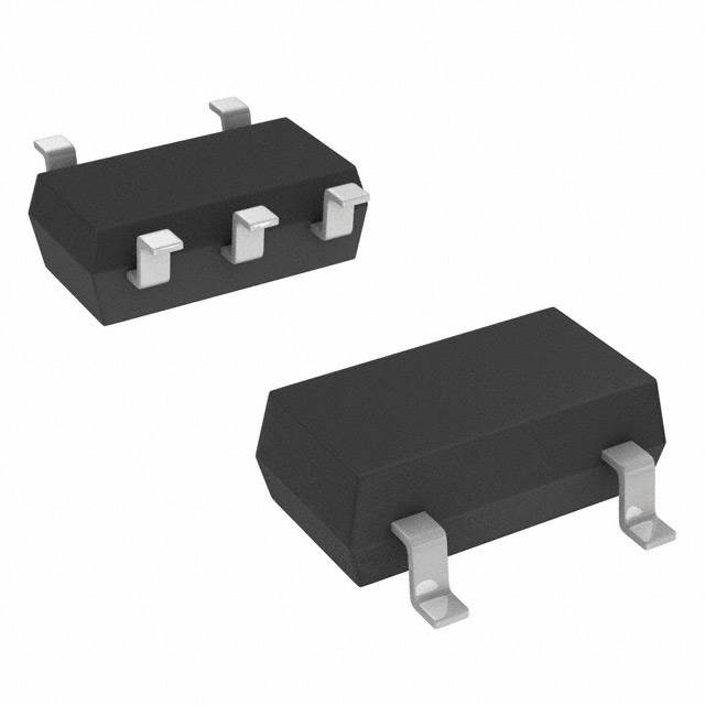
Compact Industry Standard SC70-5 Surface Mount Package
RoHS Compliant
Applications
Battery Load switch
Power management
Pin 1
SC70-5
Package Marking and Ordering Information
Device Marking
Device
Reel Size
Tape Width
Quantity
91
FDG901D
7”
8mm
3000 units
©2007 Fairchild Semiconductor Corporation
FDG901D Rev. E
1
www.fairchildsemi.com
FDG901D Slew Rate Control IC for P-Channel MOSFETs
February 2008
�FDG901D Slew Rate Control IC for P-Channel MOSFETs
Pin Configuration
G ATE
1
SLEW
2
VDD
3
5
GND
4
LOG IC IN
Absolute Maximum Ratings
Parameter
Min.
Max.
Supply Voltage
-0.5
10
V
DC Input Voltage (Logic Inputs)
-0.7
9
V
150
mW
-65
150
°C
425
°C/W
Max.
Unit
Power Dissipation for Single Operation @ 85°C
Operating and Storage Junction Temperature
Thermal Resistance, Junction to Ambient (note 1)
Unit
Recommended Operating Range
Parameter
Min.
Supply Voltage
2.7
6
V
Operating Junction Temperature
-40
150
°C
Electrical Characteristics
TA = 25°C unless otherwise noted
Parameter
Symbol
Conditions
Min.
Typ.
Max.
Units
2.0
V
Logic Levels
Logic High Input Voltage
VIH
VDD = 2.7V to 6.0V
Logic Low Input Voltage
VIL
VDD = 2.7V to 6.0V
2.55
V
Off Characteristics - Slew Rate Control Driver
Supply Input Breakdown Voltage
BVDG
IDG = 10 A, VIN = 0V, VSLEW = 0V
9
V
Slew Input Breakdown Voltage
BVSLEW
ISLEW = 10 A, VIN = 0V
9
V
Logic Input Breakdown Voltage
BVIN
IIN = 10 A, VSLEW = 0V
9
V
Supply Input Leakage Current
IRDG
VDG = 8V, VIN = 0V, VSLEW = 0V
100
nA
Slew Input Leakage Current
IRSLEW
VSLEW = 8V, VIN = 0V
100
nA
Logic Input Leakage Current
IRIN
VIN = 8V, VSLEW = 0V
100
nA
On Characteristics - Slew Rate Control Driver
Gate Current
IG
VIN = 6V,
VGATE = 2V
Slew Pin = Open
90
120
A
Slew Pin = GND
1
10
A
Slew Pin = VDD
10
50
nA
Notes: Rθ JA is the sum of the junction-to-case and case-to-ambient thermal resistance where the case thermal reference is defined
as the solder mounting surface of the drain pins. Rθ JC is guaranteed by design while Rθ CA is determined by the user's board design.
FDG901D Rev. E
2
www.fairchildsemi.com
�TA = 25°C unless otherwise noted
Parameter
Symbol
Conditions
Min.
Typ.
Max.
Units
P-Channel Switching Times (VSUPPLY = 5.5V, VDD = 5.5V, Logic IN = 5.5V, CLOAD = 510pF, Test Circuit)
Delay On Time
tdON
VOUT Rise Time
tR
= Open
8.3
s
Slew Pin = GND
0.6
ms
= VDD
2.2
ms
= Open
28
s
Slew Pin = GND
1.8
ms
11
ms
= VDD
Output Slew Rate
dv/dt
= Open
162
V/ms
Slew Pin = GND
26
V/ms
0.3
V/ms
= VDD
VDD
SLEW
2
VSUPPLY
3
L O G IC IN
CLoad
10%
90%
1
LOGIC IN
4
O U TPUT
( In v e r te d )
5
10%
td O N
tR
Test Circuit
FDG901D Rev. E
Switching Waveform
3
www.fairchildsemi.com
FDG901D Slew Rate Control IC for P-Channel MOSFETs
Electrical Characteristics Cont.
�2.0
100
Slew = Gnd
Vdd=Vin=6V
Slew = Open
Vdd=Vin=6V
95
1.5
Gate Current (µA)
Gate Current, (µA)
90
85
80
75
70
1.0
0.5
65
60
-50
0
50
100
0.0
150
-50
0
50
Temperature, (oC)
Figure 1. Gate Output Current vs. Temperature
(SLEW = OPEN)
Figure 2. Gate Output Current vs. Temperature
(SLEW = GROUND)
Output Risetime, microseconds (µsec)
Slew = Vdd
Vdd=Vin=6V
12
Gate Current, (nA)
150
100
14
10
8
6
4
-50
0
50
100
Slew = Open
Vdd=Vin=5.5V
10
1
0.1
150
1
10
o
Temperature, ( C)
10000
100
1000
Load Capacitance, picoFarad (pF)
Figure 3. Gate Output Current vs. Temperature
(SLEW = VDD)
Figure 4. tRISE vs. Load Capacitance
(SLEW = OPEN)
100
Slew = Gnd
Vdd=Vin=5.5V
Output Risetime, milliseconds (ms)
Output Risetime, microseconds (µs)
100
Temperature, (oC)
1000
100
10
1
Slew = Vdd
Vdd=Vin=5.5V
10
1
0.1
1
10
100
1000
1
Load Capacitance, picoFarad (pF)
Figure 5. tRISE vs. Load Capacitance
(SLEW = GROUND)
FDG901D Rev. E
10
100
1000
Load Capacitance, picoFarad (pF)
Figure 6. tRISE vs. Load Capacitance
(SLEW = VDD)
4
www.fairchildsemi.com
FDG901D Slew Rate Control IC for P-Channel MOSFETs
Typical Characteristics
�160
7.5
Slew = Open
Vdd=Vin=5.5V
7.0
120
6.5
time, µsecs
time, microseconds (µs)
Slew = Gnd
Vdd=Vin=5.5V
140
trise
6.0
tdon
5.5
trise
100
80
tdon
60
40
20
5.0
0
10
20
30
40
0
50
0
Load Resistance, ohms (Ω)
10
20
30
40
50
Load Resistance, ohms (Ω)
Figure 7. Switching Time vs. Load Resistance
(SLEW = OPEN)
Figure 8. Switching Time vs. Load Resistance
(SLEW = GROUND)
200
7.5
Slew = Vdd
Vdd=Vin=5.5V
Slew = Open
Vdd=Vin=5.5V
7.0
150
time, ( µsec)
time, microseconds (µs)
175
tris
125
trise
6.5
tdon
6.0
tdon
100
5.5
75
5.0
0
10
20
30
40
50
0.0
0.5
1.0
2.0
2.5
Figure 10. Switching Time vs. Load Current
(SLEW = OPEN)
Figure 9. Switching Time vs. Load Resistance
(SLEW = VDD)
160
200
Slew = Gnd
Vdd=Vin=5.5V
140
1.5
Load Current, Amps (A)
Load Resistance, ohms (Ω)
Slew = Vdd
Vdd=Vin=5.5V
time, µsec
time, microseconds (µs)
175
120
trise
100
80
60
tdon
trise
150
125
tdon
100
40
20
75
0.0
0.5
1.0
1.5
2.0
2.5
0.0
Load Current, Amps (A)
1.0
1.5
2.0
2.5
Load Current, Amps (A)
Figure 11. Switching Time vs. Load Current
(SLEW = GROUND)
FDG901D Rev. E
0.5
Figure 12. Switching Time vs. Load Current
(SLEW = VDD)
5
www.fairchildsemi.com
FDG901D Slew Rate Control IC for P-Channel MOSFETs
Typical Characteristics
�FDG901D Slew Rate Control IC for P-Channel MOSFETs
Application Information
Typical Application
I
Source
Drain
Gate
VDD
Logic
Signal
Slew Rate
Control
3
4
Load
1
2
Ig
5
Application Circuit
Battery powered systems make extensive usage of load
switching, turning the power to subsystems off, in order to
extend battery life. Power MOSFETs are used to accomplish
this task. In PDA's and Cell phones, these MOSFETs are
usually low threshold P-Channels. Since the loads typically
include bypass capacitor components (high capacitive
component), a high inrush current can occur when the load is
switched on. This inrush current can cause transients on the
main power supply disturbing circuitry supplied by it.
t=
IG
where Qg is the Gate charge in nC for a given MOSFET and IG
is the gate current controlled by the slew rate pin.
The simplest method of limiting the inrush current is to control
the slew rate of the MOSFET switch. This can be done with
external R/C circuits, but this approach can occupy significant
PCB area, and involves other compromises in performance.
The slew rate control driver IC FDG901D is specifically
designed to interface low voltage digital circuitry with power
MOSFETs and reduce the rapid inrush current in load switch
applications. The IC limits inrush current by controlling the
current, which drives the gate of the P-Channel MOSFET
switch.
Below is a captured image from an oscilloscope depicting the
device response. The FDG901D was connected to control an
FDG258P P-Channel DMOS. The Slew Rate control pin was
set to open (floating state).
The control input is a CMOS compatible input with a minimum
high input voltage of 2.55V with a power rail voltage of 6V.
Therefore, it is compatible with any CMOS logic voltages
between 2.55V and 5V and under these conditions there is no
additional configuration required.
V IN
V
The Slew Rate Control Driver (FDG901D) is designed to give a
programmed choice of one of three steady dv/dt states on the
output during turn-on. To change the dv/dt value, the user
needs to use the Slew Rate Control Pin (Pin 2). To utilize the
smallest current setting ( 10 nA) from the IC, a voltage equal to
VDD must be applied to the Slew Rate Control Pin 2. To use the
next higher current setting ( ~1 A) a voltage equal to Ground
must be applied to Pin 2. To achieve the highest current setting
( ~80 A) or obtain a faster switching speed, the Slew Rate Pin2
must be open (floating). A higher value of capacitance will
result in a slower switching rate. To determine the switching
times of each setting use the simple equation:
FDG901D Rev. E
Qg
gate
(inverted)
V RLoad
V DD = 5.5V
V IN = 5.5V
R LOAD = 1.5
Circuit w aveform s for an FDG901D controlling a P-Channel FDG 258P MO FET
6
www.fairchildsemi.com
�FDG901D Slew Rate Control IC for P-Channel MOSFETs
Dimensional Outline and Pad Layout
FDG901D Rev. E
7
www.fairchildsemi.com
�TRADEMARKS
The following includes registered and unregistered trademarks and service marks, owned by Fairchild Semiconductor and/or its global
subsidiaries, and is not intended to be an exhaustive list of all such trademarks.
ACEx®
Build it Now™
CorePLUS™
CROSSVOLT™
CTL™
Current Transfer Logic™
EcoSPARK®
EZSWITCH™ *
™
FPS™
FRFET®
Global Power ResourceSM
Green FPS™
Green FPS™ e-Series™
GTO™
i-Lo™
IntelliMAX™
ISOPLANAR™
MegaBuck™
MICROCOUPLER™
MicroFET™
MicroPak™
MillerDrive™
Motion-SPM™
OPTOLOGIC®
OPTOPLANAR®
®
Fairchild®
Fairchild Semiconductor®
FACT Quiet Series™
FACT®
FAST®
FastvCore™
FlashWriter® *
®
PDP-SPM™
Power220®
POWEREDGE®
Power-SPM™
PowerTrench®
Programmable Active Droop™
QFET®
QS™
QT Optoelectronics™
Quiet Series™
RapidConfigure™
SMART START™
SPM®
STEALTH™
SuperFET™
SuperSOT™-3
SuperSOT™-6
SuperSOT™-8
SupreMOS™
SyncFET™
®
The Power Franchise®
TinyBoost™
TinyBuck™
TinyLogic®
TINYOPTO™
TinyPower™
TinyPWM™
TinyWire™
μSerDes™
UHC®
Ultra FRFET™
UniFET™
VCX™
* EZSWITCH™ and FlashWriter® are trademarks of System General Corporation, used under license by Fairchild Semiconductor.
DISCLAIMER
FAIRCHILD SEMICONDUCTOR RESERVES THE RIGHT TO MAKE CHANGES WITHOUT FURTHER NOTICE TO ANY PRODUCTS
HEREIN TO IMPROVE RELIABILITY, FUNCTION, OR DESIGN. FAIRCHILD DOES NOT ASSUME ANY LIABILITY ARISING OUT OF THE
APPLICATION OR USE OF ANY PRODUCT OR CIRCUIT DESCRIBED HEREIN; NEITHER DOES IT CONVEY ANY LICENSE UNDER ITS
PATENT RIGHTS, NOR THE RIGHTS OF OTHERS. THESE SPECIFICATIONS DO NOT EXPAND THE TERMS OF FAIRCHILD’S
WORLDWIDE TERMS AND CONDITIONS, SPECIFICALLY THE WARRANTY THEREIN, WHICH COVERS THESE PRODUCTS.
LIFE SUPPORT POLICY
FAIRCHILD’S PRODUCTS ARE NOT AUTHORIZED FOR USE AS CRITICAL COMPONENTS IN LIFE SUPPORT DEVICES OR
SYSTEMS WITHOUT THE EXPRESS WRITTEN APPROVAL OF FAIRCHILD SEMICONDUCTOR CORPORATION.
As used herein:
1. Life support devices or systems are devices or systems
which, (a) are intended for surgical implant into the body or
(b) support or sustain life, and (c) whose failure to perform
when properly used in accordance with instructions for use
provided in the labeling, can be reasonably expected to
result in a significant injury of the user.
2. A critical component in any component of a life support,
device, or system whose failure to perform can be
reasonably expected to cause the failure of the life support
device or system, or to affect its safety or effectiveness.
PRODUCT STATUS DEFINITIONS
Definition of Terms
Datasheet Identification
Product Status
Definition
Advance Information
Formative or In Design
This datasheet contains the design specifications for product
development. Specifications may change in any manner without notice.
Preliminary
First Production
This datasheet contains preliminary data; supplementary data will be
published at a later date. Fairchild Semiconductor reserves the right to
make changes at any time without notice to improve design.
No Identification Needed
Full Production
This datasheet contains final specifications. Fairchild Semiconductor
reserves the right to make changes at any time without notice to improve
the design.
Obsolete
Not In Production
This datasheet contains specifications on a product that has been
discontinued by Fairchild Semiconductor. The datasheet is printed for
reference information only.
Rev. I33
© 2008 Fairchild Semiconductor Corporation
www.fairchildsemi.com
�