Is Now Part of
To learn more about ON Semiconductor, please visit our website at
www.onsemi.com
ON Semiconductor and the ON Semiconductor logo are trademarks of Semiconductor Components Industries, LLC dba ON Semiconductor or its subsidiaries in the United States and/or other countries. ON Semiconductor owns the rights to a number
of patents, trademarks, copyrights, trade secrets, and other intellectual property. A listing of ON Semiconductor’s product/patent coverage may be accessed at www.onsemi.com/site/pdf/Patent-Marking.pdf. ON Semiconductor reserves the right
to make changes without further notice to any products herein. ON Semiconductor makes no warranty, representation or guarantee regarding the suitability of its products for any particular purpose, nor does ON Semiconductor assume any liability
arising out of the application or use of any product or circuit, and specifically disclaims any and all liability, including without limitation special, consequential or incidental damages. Buyer is responsible for its products and applications using ON
Semiconductor products, including compliance with all laws, regulations and safety requirements or standards, regardless of any support or applications information provided by ON Semiconductor. “Typical” parameters which may be provided in ON
Semiconductor data sheets and/or specifications can and do vary in different applications and actual performance may vary over time. All operating parameters, including “Typicals” must be validated for each customer application by customer’s
technical experts. ON Semiconductor does not convey any license under its patent rights nor the rights of others. ON Semiconductor products are not designed, intended, or authorized for use as a critical component in life support systems or any FDA
Class 3 medical devices or medical devices with a same or similar classification in a foreign jurisdiction or any devices intended for implantation in the human body. Should Buyer purchase or use ON Semiconductor products for any such unintended
or unauthorized application, Buyer shall indemnify and hold ON Semiconductor and its officers, employees, subsidiaries, affiliates, and distributors harmless against all claims, costs, damages, and expenses, and reasonable attorney fees arising out
of, directly or indirectly, any claim of personal injury or death associated with such unintended or unauthorized use, even if such claim alleges that ON Semiconductor was negligent regarding the design or manufacture of the part. ON Semiconductor
is an Equal Opportunity/Affirmative Action Employer. This literature is subject to all applicable copyright laws and is not for resale in any manner.
�FDH300 / FDH300A / FDLL300A / FDH333 / FDLL333
High Conductance Low Leakage Diode
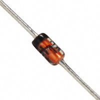
Cathode Band
LL-34 COLOR BAND MARKING
DEVICE
FDLL300A
FDLL333
WHITE
WHITE
-1st band denotes cathode terminal
and has wider width
LL-34 (SOD-80)
DO-35
1ST BAND
THE PLACEMENT OF THE EXPANSION GAP
HAS NO RELATIONSHIP TO THE LOCATION
OF THE CATHODE TERMINAL
Cathode is denoted with a black band
Ordering Information
Part Number
Top Mark
Package
Packing Method
FDH300TR
H300
DO-204AH (DO-35)
Tape and Reel
FDH300A
H300A
DO-204AH (DO-35)
Bulk
FDH300ATR
H300A
DO-204AH (DO-35)
Tape and Reel
FDH333
H333
DO-204AH (DO-35)
Bulk
FDH333TR
H333
DO-204AH (DO-35)
Tape and Reel
FDLL300A
WHITE
SOD-80 2L
Tape and Reel
FDLL333
WHITE
SOD-80 2L
Tape and Reel
Absolute Maximum Ratings(1), (2)
Stresses exceeding the absolute maximum ratings may damage the device. The device may not function or be operable above the recommended operating conditions and stressing the parts to these levels is not recommended. In addition, extended exposure to stresses above the recommended operating conditions may affect device reliability. The
absolute maximum ratings are stress ratings only. Values are at TA = 25°C unless otherwise noted.
Symbol
WIV
Parameter
Value
Unit
Working Inverse Voltage
125
V
IO
Average Rectified Forward Current
200
mA
IF
DC Forward Current
500
mA
if
Recurrent Peak Forward Current
600
mA
IFSM
Non-Repetitive Peak Forward
Surge Current
TSTG
Storage Temperature Range
TJ
Operating Junction Temperature
Pulse Width = 1.0 s
1.0
Pulse Width = 1.0 s
4.0
A
-65 to +200
°C
175
°C
Notes:
1. These ratings are based on a maximum junction temperature of 175C.
2. These are steady-state limits. Fairchild Semiconductor should be consulted on applications involving pulsed or
low-duty-cycle operations.
© 1997 Fairchild Semiconductor Corporation
FDH300 / FDH300A / FDLL300A / FDH333 / FDLL333 Rev. 3.4
www.fairchildsemi.com
FDH300 / FDH300A / FDLL300A / FDH333 / FDLL333 — High Conductance Low Leakage Diode
February 2016
�Values are at TA = 25°C unless otherwise noted.
Symbol
PD
RJA
Parameter
Max.
Unit
Total Device Dissipation
500
mW
Derate Above 25°C
3.33
mW/C
Thermal Resistance, Junction-to-Ambient
300
C/W
Electrical Characteristics
Values are at TA = 25°C unless otherwise noted.
Symbol
VR
VF
Parameter
Conditions
IR = 100 A
Breakdown Voltage
Forward Voltage
150
Unit
V
680
mV
FDH300
IF = 5.0 mA
750
mV
FDH300A / FDLL300A
IF = 5.0 mA
760
mV
FDH300 / FDH300A / FDLL300A IF = 10 mA
800
mV
FDH300
IF = 50 mA
880
mV
FDH300A / FDLL300A
IF = 50 mA
890
mV
920
mV
FDH300 / FDH300A / FDLL300A IF = 100 mA
FDH300 / FDH300A / FDLL300A IF = 200 mA
FDH300 / FDH300A / FDLL300A
Reverse Current
FDH333 / FDLL333
CO
Max.
FDH300 / FDH300A / FDLL300A IF = 1.0 mA
FDH333 / FDLL333
IR
Min.
Diode Capacitance
© 1997 Fairchild Semiconductor Corporation
FDH300 / FDH300A / FDLL300A / FDH333 / FDLL333 Rev. 3.4
1.0
V
IF = 50 mA
800
890
mV
IF = 100 mA
830
940
mV
IF = 150 mA
860
970
mV
IF = 200 mA
0.87
1.05
V
IF = 250 mA
0.88
1.08
V
IF = 300 mA
0.90
1.15
V
VR = 125 V
1.0
nA
VR = 125 V, TA = 150°C
3.0
A
VR = 125 V
3.0
nA
VR = 125 V, TA = 100°C
500
nA
VR = 0, f = 1.0 MHz
6.0
pF
www.fairchildsemi.com
2
FDH300 / FDH300A / FDLL300A / FDH333 / FDLL333 — High Conductance Low Leakage Diode
Thermal Characteristics
�0.50
0.30
1.50
1.30
2.64 REF
1.40
1.20
C
0.30
R
0.20
3.60
3.30
3.30
0.50
1.65
1.10
0.50
LAND PATTERN RECOMMENDATION
NOTES: UNLESS OTHERWISE SPECIFIED
A) PACKAGE STANDARD REFERENCE:
JEDEC DO-213, VARIATION AC.
B) ALL DIMENSIONS ARE IN MILLIMETERS.
C
CORNER RADIUS IS OPTIONAL.
D) LAND PATTERN RECOMMENDATION PER IPC DIOMELF3414N
E) DRAWING FILE NAME: SOD80A
REV3
�T50 = 25.40 MIN (2X)
T26 = 14.00 MIN (2X)
4.56
3.05
0.533
0.460
NOTES: UNLESS OTHERWISE SPECIFIED
A) PACKAGE STANDARD REFERENCE:
JEDEC DO-204, VARIATION AH.
B) HERMETICALLY SEALED GLASS PACKAGE.
C) PACKAGE WEIGHT IS 0.137 GRAM.
D) ALL DIMENSIONS ARE IN MILLIMETERS.
E) DRAWING FILE NAME: DO35AREV03
1.91
1.53
�ON Semiconductor and
are trademarks of Semiconductor Components Industries, LLC dba ON Semiconductor or its subsidiaries in the United States and/or other countries.
ON Semiconductor owns the rights to a number of patents, trademarks, copyrights, trade secrets, and other intellectual property. A listing of ON Semiconductor’s product/patent
coverage may be accessed at www.onsemi.com/site/pdf/Patent−Marking.pdf. ON Semiconductor reserves the right to make changes without further notice to any products herein.
ON Semiconductor makes no warranty, representation or guarantee regarding the suitability of its products for any particular purpose, nor does ON Semiconductor assume any liability
arising out of the application or use of any product or circuit, and specifically disclaims any and all liability, including without limitation special, consequential or incidental damages.
Buyer is responsible for its products and applications using ON Semiconductor products, including compliance with all laws, regulations and safety requirements or standards,
regardless of any support or applications information provided by ON Semiconductor. “Typical” parameters which may be provided in ON Semiconductor data sheets and/or
specifications can and do vary in different applications and actual performance may vary over time. All operating parameters, including “Typicals” must be validated for each customer
application by customer’s technical experts. ON Semiconductor does not convey any license under its patent rights nor the rights of others. ON Semiconductor products are not
designed, intended, or authorized for use as a critical component in life support systems or any FDA Class 3 medical devices or medical devices with a same or similar classification
in a foreign jurisdiction or any devices intended for implantation in the human body. Should Buyer purchase or use ON Semiconductor products for any such unintended or unauthorized
application, Buyer shall indemnify and hold ON Semiconductor and its officers, employees, subsidiaries, affiliates, and distributors harmless against all claims, costs, damages, and
expenses, and reasonable attorney fees arising out of, directly or indirectly, any claim of personal injury or death associated with such unintended or unauthorized use, even if such
claim alleges that ON Semiconductor was negligent regarding the design or manufacture of the part. ON Semiconductor is an Equal Opportunity/Affirmative Action Employer. This
literature is subject to all applicable copyright laws and is not for resale in any manner.
PUBLICATION ORDERING INFORMATION
LITERATURE FULFILLMENT:
Literature Distribution Center for ON Semiconductor
19521 E. 32nd Pkwy, Aurora, Colorado 80011 USA
Phone: 303−675−2175 or 800−344−3860 Toll Free USA/Canada
Fax: 303−675−2176 or 800−344−3867 Toll Free USA/Canada
Email: orderlit@onsemi.com
© Semiconductor Components Industries, LLC
N. American Technical Support: 800−282−9855 Toll Free
USA/Canada
Europe, Middle East and Africa Technical Support:
Phone: 421 33 790 2910
Japan Customer Focus Center
Phone: 81−3−5817−1050
www.onsemi.com
1
ON Semiconductor Website: www.onsemi.com
Order Literature: http://www.onsemi.com/orderlit
For additional information, please contact your local
Sales Representative
www.onsemi.com
�


 工商网监
湘ICP备2023018690号
工商网监
湘ICP备2023018690号
