FDP045N10A / FDI045N10A
MOSFET – N-Channel,
POWERTRENCH)
100 V, 164 A, 4.5 mW
www.onsemi.com
Description
This N−Channel MOSFET is produced using ON Semiconductor’s
advance POWERTRENCH process that has been tailored to minimize
the on−state resistance while maintaining superior switching
performance.
D
Features
•
•
•
•
•
•
RDS(on) = 3.8 mW ( Typ.) @ VGS = 10 V, ID = 100 A
Fast Switching Speed
Low Gate Charge, QG = 54 nC (Typ.)
High Performance Trench Technology for Extremely Low RDS(on)
High Power and Current Handling Capability
This Device is Pb−Free and is RoHS Compliant
G
S
Applications
•
•
•
•
Synchronous Rectification for ATX / Server / Telecom PSU
Battery Protection Circuit
Motor Drives and Uninterruptible Power Supplies
Micro Solar Inverter
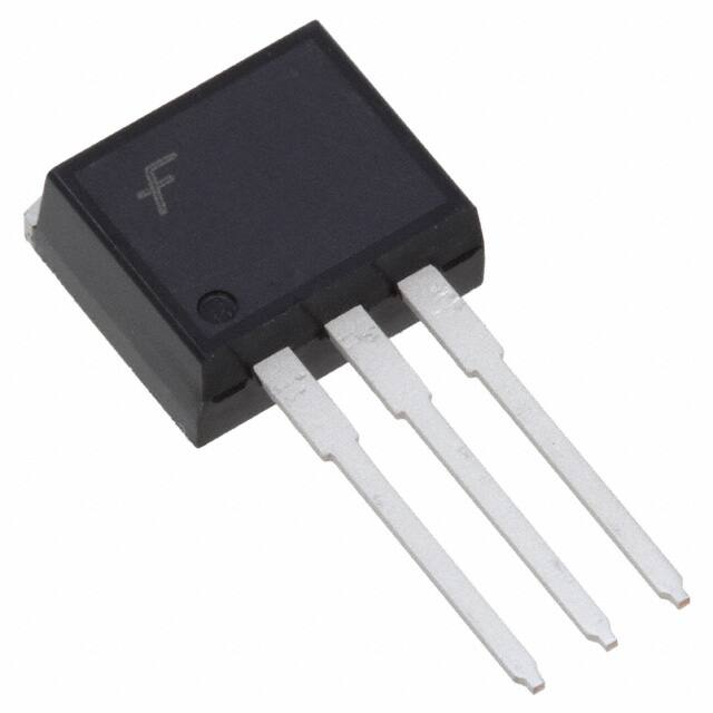
TO−220
CASE 221A−09
I2PAK
CASE 418AV
MARKING DIAGRAM
$Y&Z&3&K
FDP
045N10A
$Y
&Z
&3
&K
FDP/FDI045N10A
$Y&Z&3&K
FDI
045N10A
= ON Semiconductor Logo
= Assembly Plant Code
= Numeric Date Code
= Lot Code
= Specific Device Code
ORDERING INFORMATION
See detailed ordering and shipping information on page 2 of
this data sheet.
© Semiconductor Components Industries, LLC, 2011
June, 2019 − Rev. 3
1
Publication Order Number:
FDP045N10A/D
�FDP045N10A / FDI045N10A
MOSFET MAXIMUM RATINGS (TC = 25°C Unless Otherwise Noted)
Symbol
Parameter
FDP045N10A_F102
FDI045N10A_F102
Unit
VDSS
Drain to Source Voltage
100
V
VGSS
Gate to Source Voltage
±20
V
− Continuous (TC = 25°C, Silicon Limited)
164*
A
− Continuous (TC = 100°C, Silicon LImited)
116
− Continuous (TC = 25°C, Package Limited)
120
− Pulsed (Note 1)
656
A
637
mJ
ID
Drain Current
IDM
Drain Current
EAS
Single Pulsed Avalanche Energy (Note 2)
dv/dt
Peak Diode Recovery dv/dt (Note 3)
6.0
V/ns
Power Dissipation
(TC = 25°C)
263
W
− Derate Above 25°C
1.75
W/°C
−55 to +175
°C
300
°C
PD
Operating and Storage Temperature Range
TJ, TSTG
Maximum Lead Temperature for Soldering, 1/8” from Case for 5 Seconds
TL
Stresses exceeding those listed in the Maximum Ratings table may damage the device. If any of these limits are exceeded, device functionality
should not be assumed, damage may occur and reliability may be affected.
*Calculated continuous current based on maximum allowable junction temperature. Package limitation current is 120 A.
THERMAL CHARACTERISTICS
Symbol
Parameter
FDP045N10A_F102
FDI045N10A_F102
Unit
°C
RθJC
Thermal Resistance, Junction to Case, Max.
0.57
RθJA
Thermal Resistance, Junction to Ambient, Max.
62.5
PACKAGE MARKING AND ORDERING INFORMATION
Part Number
Top Mark
Package
Packing Method
Reel Size
Tape Width
Quantity
FDP045N10A_F102
FDP045N10A
TO−220
Tube
N/A
N/A
50 Units
FDI045N10A
I2−PAK
Tube
N/A
N/A
50 Units
FDI045N10A_F102
ELECTRICAL CHARACTERISTICS (TC = 25°C Unless Otherwise Noted)
Symbol
Parameter
Test Conditions
Min.
Typ.
Max.
Unit
100
−
−
V
OFF CHARACTERISTICS
Drain to Source Breakdown Voltage
ID = 250 mA, VGS = 0 V
DBVDSS
/ DTJ
Breakdown Voltage Temperature
Coefficient
ID = 250 mA, Referenced to 25°C
−
0.07
−
V/°C
IDSS
Zero Gate Voltage Drain Current
VDS = 80 V, VGS = 0 V
−
−
1
mA
VDS = 80 V, TC = 150°C
−
−
500
VGS = ±20 V, VDS = 0 V
−
−
±100
nA
2.0
−
4.0
V
BVDSS
IGSS
Gate to Body Leakage Current
ON CHARACTERISTICS
VGS(th)
Gate Threshold Voltage
VGS = VDS, ID = 250 mA
RDS(on)
Static Drain to Source On Resistance
VGS = 10 V, ID = 100 A
−
3.8
4.5
mW
Forward Transconductance
VDS = 10 V, ID = 100 A
−
132
−
S
gFS
www.onsemi.com
2
�FDP045N10A / FDI045N10A
ELECTRICAL CHARACTERISTICS (TC = 25°C Unless Otherwise Noted) (continued)
Symbol
Parameter
Test Conditions
Min.
Typ.
Max.
Unit
−
3960
5270
pF
−
925
1230
pF
−
34
−
pF
DYNAMIC CHARACTERISTICS
Ciss
Input Capacitance
Coss
Output Capacitance
Crss
Reverse Transfer Capacitance
VDS = 50 V, VGS = 0 V
f = 1 MHz
Coss(er)
Engry Releted Output Capacitance
VDS = 50 V, VGS = 0 V
−
1520
−
pF
Qg(tot)
Total Gate Charge at 10V
VGS = 10 V, VDS = 50 V,
ID = 100 A
(Note 4)
−
54
74
nC
−
17
−
nC
Qgs
Gate to Source Gate Charge
Qgs2
Gate Charge Threshold to Plateau
−
8
−
nC
Qgd
Gate to Drain “Miller” Charge
−
13
−
nC
ESR
Equivalent Series Resistance (G−S)
f = 1 MHz
−
1.9
−
W
VDD = 50 V, ID = 100 A,
VGS = 10 V, RG = 4.7 W
(Note 4)
−
23
56
ns
−
26
62
ns
−
50
110
ns
−
15
40
ns
Maximum Continuous Drain to Source Diode Forward Current
−
−
164*
A
ISM
Maximum Pulsed Drain to Source Diode Forward Current
−
−
656
A
VSD
Drain to Source Diode Forward Voltage
VGS = 0 V, ISD = 100 A
−
−
1.3
V
trr
Reverse Recovery Time
−
75
−
ns
Qrr
Reverse Recovery Charge
VGS = 0 V, VDD = 50 V,
ISD = 100 A,
dIF/dt = 100 A/ms
−
120
−
nC
SWITCHING CHARACTERISTICS
td(on)
Turn−On Delay Time
tr
Turn−On Rise Time
td(off)
Turn−Off Delay Time
tf
Turn−Off Fall Time
DRAIN−SOURCE DIODE CHARACTERISTICS
IS
Product parametric performance is indicated in the Electrical Characteristics for the listed test conditions, unless otherwise noted. Product
performance may not be indicated by the Electrical Characteristics if operated under different conditions.
1. Repetitive rating: pulse−width limited by maximum junction temperature.
2. L = 3 mH, IAS = 20.6 A, RG = 25 W, starting TJ = 25°C.
3. ISD ≤ 100 A, di/dt v 200 A/ms, VDD ≤ BVDSS, starting TJ = 25°C.
4. Essentially independent of operating temperature typical characteristics.
www.onsemi.com
3
�FDP045N10A / FDI045N10A
TYPICAL PERFORMANCE CHARACTERISTICS
500
VGS = 15.0 V
10.0 V
8.0 V
6.5 V
6.0 V
5.5 V
5.0 V
100
ID, Drain Current [A]
ID, Drain Current [A]
500
100
1
10
−55°C
1
2
1
VDS, Drain−Source Voltage [V]
3
4
5
6
Figure 2. Transfer Characteristics
4.5
500
IS, Reverse Drain Current [A]
RDS(ON) [mW],
Drain−Source On−Resistance
2
VGS, Gate−Source Voltage [V]
Figure 1. On−Region Characteristics
VGS = 10 V
4.0
VGS = 20 V
3.5
3.0
25°C
175°C
*Notes:
1. 250 ms Pulse Test
2. TC = 25°C
10
0.1
*Notes:
1. VDS = 10 V
2. 250 ms Pulse Test
100
*Note: TC = 25°C
0
100
200
300
175°C
25°C
10
1
0.0
400
*Notes:
1. VGS = 0 V
2. 250 ms Pulse Test
0.3
0.6
0.9
1.2
1.5
ID, Drain Current [A]
VSD, Body Diode Forward Voltage [V]
Figure 3. On−Resistance Variation vs.
Drain Current and Gate Voltage
Figure 4. Body Diode Forward Voltage
Variation vs. Source Current and Temperature
10
10000
VGS, Gate−Source Voltage [V]
Capacitances [pF]
Ciss
1000
Coss
Crss
Note:
1. VGS = 0 V
2. f = 1 MHz
100
Ciss = Cgs + Cgd (Cds = shorted)
Coss = Cds + Cgd
Crss = Cgd
10
0.1
1
10
6
4
2
0
100
VDS, Drain−Source Voltage [V]
VDS = 20 V
VDS = 50 V
VDS = 80 V
8
*Note: ID = 100 A
0
10
20
30
40
50
Qg, Total Gate Charge [nC]
Figure 5. Capacitance Characteristics
Figure 6. Gate Charge Characteristics
www.onsemi.com
4
60
�FDP045N10A / FDI045N10A
TYPICAL PERFORMANCE CHARACTERISTICS (continued)
2.5
RDS(on), [Normalized]
Drain−Source On−Resistance
BVDSS, [Normalized]
Drain−Source Breakdown Voltage
1.10
1.05
1.00
0.95
0.90
−100
*Notes:
1. VGS = 0 V
2. ID = 250 mA
−50
0
50
100
150
1.5
1.0
0.5
0.0
−100
200
−50
0
50
100
150
200
TJ, Junction Temperature (°C)
Figure 7. Maximum Safe Operating Area
Figure 8. On−Resistance Variation vs.
Temperature
175
150
100 ms
125
10
1 ms
Operation in This Area
is Limited by RDS(on)
1
VGS = 10 V
30 ms
ID, Drain Current (A)
100
10ms
*Notes:
1. TC = 25°C
2. TJ = 175°C
3. Single Pulse
0.1
0.1
1
DC
100
75
50
25
10
RqJC = 0.57°C/W
0
25
100200
50
75
100
125
150
175
VDS, Drain−Source Voltage [V]
TC, Case Temperature (°C)
Figure 9. Maximum Safe Operating Area
Figure 10. Maximum Drain Current
vs. Case Temperature
5
50
IAS, Avalanche Current [A]
4
EOSS, [mJ]
*Notes:
1. VGS = 10 V
2. ID = 100 A
TJ, Junction Temperature (°C)
1000
ID, Drain Current [A]
2.0
3
2
1
0
0
25
50
75
If R = 0
tAV = (L)(IAS)/(1.3×RATED BVDSS−VDD)
If R = 0
tAV = (L/R)In[(IAS×R)/(1.3×RATED BVDSS−VDD)+1]
Starting TJ = 150°C
1
0.01
100
Starting TJ = 25°C
10
0.1
1
10
100
1000
VDS, Drain to Source Voltage [V]
tAV, Time In Avalanche [ms]
Figure 11. Eoss vs. Drain to Source Voltage
Figure 12. Unclamped Inductive
Switching Capability
www.onsemi.com
5
�FDP045N10A / FDI045N10A
TYPICAL PERFORMANCE CHARACTERISTICS (continued)
ZqJC(t), Thermal Response [°C/W]
1
0.5
0.1
0.2
0.1
P DM
0.05
t1
0.02
0.01
0.01
Single pulse
0.001
−5
10
t2
Notes:
1. ZqJC(t) = 0.57°C/W Max.
2. Duty Factor, D= t1/t2
3. TJM − TC = PDM × ZqJC(t)
−4
10
−3
−2
10
10
−1
10
t, Rectangular Pulse Duration [sec]
Figure 13. Transient Thermal Response Curve
Figure 14. Gate Charge Test Circuit & Waveform
www.onsemi.com
6
1
�FDP045N10A / FDI045N10A
VDS
RG
V
10V
GS
RL
VDS
90%
VDD
VGS
VGS
DUT
10%
td(on)
tr
td(off)
t on
Figure 15. Resistive Switching Test Circuit & Waveforms
Figure 16. Unclamped Inductive Switching Test Circuit & Waveforms
www.onsemi.com
7
t off
tf
�FDP045N10A / FDI045N10A
DUT
+
VDS
_
I SD
L
Driver
RG
VGS
VGS
( Driver )
I SD
( DUT )
Same Type
as DUT
VDD
Sdv/dtcontrolled by RG
SI SD controlled by pulse period
D = −−−−−−−−−−−−−−−−−−−−−−−−−−
10V
IFM , Body Diode Forward Current
di/dt
IRM
Body Diode Reverse Current
VDS
( DUT )
Body Diode Recoverydv/dt
VDD
VSD
Body Diode
Forward Voltage Drop
Figure 17. Peak Diode Recovery dv/dt Test Circuit & Waveforms
POWERTRENCH is registered trademarks of Semiconductor Components Industries, LLC (SCILLC) or its subsidiaries in the United States and/or other
countries.
www.onsemi.com
8
�MECHANICAL CASE OUTLINE
PACKAGE DIMENSIONS
TO−220
CASE 221A−09
ISSUE AJ
DATE 05 NOV 2019
SCALE 1:1
STYLE 1:
PIN 1.
2.
3.
4.
BASE
COLLECTOR
EMITTER
COLLECTOR
STYLE 2:
PIN 1.
2.
3.
4.
BASE
EMITTER
COLLECTOR
EMITTER
STYLE 3:
PIN 1.
2.
3.
4.
CATHODE
ANODE
GATE
ANODE
STYLE 4:
PIN 1.
2.
3.
4.
MAIN TERMINAL 1
MAIN TERMINAL 2
GATE
MAIN TERMINAL 2
STYLE 5:
PIN 1.
2.
3.
4.
GATE
DRAIN
SOURCE
DRAIN
STYLE 6:
PIN 1.
2.
3.
4.
ANODE
CATHODE
ANODE
CATHODE
STYLE 7:
PIN 1.
2.
3.
4.
CATHODE
ANODE
CATHODE
ANODE
STYLE 8:
PIN 1.
2.
3.
4.
CATHODE
ANODE
EXTERNAL TRIP/DELAY
ANODE
STYLE 9:
PIN 1.
2.
3.
4.
GATE
COLLECTOR
EMITTER
COLLECTOR
STYLE 10:
PIN 1.
2.
3.
4.
GATE
SOURCE
DRAIN
SOURCE
STYLE 11:
PIN 1.
2.
3.
4.
DRAIN
SOURCE
GATE
SOURCE
STYLE 12:
PIN 1.
2.
3.
4.
MAIN TERMINAL 1
MAIN TERMINAL 2
GATE
NOT CONNECTED
DOCUMENT NUMBER:
DESCRIPTION:
98ASB42148B
TO−220
Electronic versions are uncontrolled except when accessed directly from the Document Repository.
Printed versions are uncontrolled except when stamped “CONTROLLED COPY” in red.
PAGE 1 OF 1
ON Semiconductor and
are trademarks of Semiconductor Components Industries, LLC dba ON Semiconductor or its subsidiaries in the United States and/or other countries.
ON Semiconductor reserves the right to make changes without further notice to any products herein. ON Semiconductor makes no warranty, representation or guarantee regarding
the suitability of its products for any particular purpose, nor does ON Semiconductor assume any liability arising out of the application or use of any product or circuit, and specifically
disclaims any and all liability, including without limitation special, consequential or incidental damages. ON Semiconductor does not convey any license under its patent rights nor the
rights of others.
© Semiconductor Components Industries, LLC, 2019
www.onsemi.com
�MECHANICAL CASE OUTLINE
PACKAGE DIMENSIONS
I2PAK (TO−262 3 LD)
CASE 418AV
ISSUE O
DOCUMENT NUMBER:
DESCRIPTION:
98AON13814G
I2PAK (TO−262 3 LD)
DATE 30 SEP 2016
Electronic versions are uncontrolled except when accessed directly from the Document Repository.
Printed versions are uncontrolled except when stamped “CONTROLLED COPY” in red.
PAGE 1 OF 1
ON Semiconductor and
are trademarks of Semiconductor Components Industries, LLC dba ON Semiconductor or its subsidiaries in the United States and/or other countries.
ON Semiconductor reserves the right to make changes without further notice to any products herein. ON Semiconductor makes no warranty, representation or guarantee regarding
the suitability of its products for any particular purpose, nor does ON Semiconductor assume any liability arising out of the application or use of any product or circuit, and specifically
disclaims any and all liability, including without limitation special, consequential or incidental damages. ON Semiconductor does not convey any license under its patent rights nor the
rights of others.
© Semiconductor Components Industries, LLC, 2019
www.onsemi.com
�onsemi,
, and other names, marks, and brands are registered and/or common law trademarks of Semiconductor Components Industries, LLC dba “onsemi” or its affiliates
and/or subsidiaries in the United States and/or other countries. onsemi owns the rights to a number of patents, trademarks, copyrights, trade secrets, and other intellectual property.
A listing of onsemi’s product/patent coverage may be accessed at www.onsemi.com/site/pdf/Patent−Marking.pdf. onsemi reserves the right to make changes at any time to any
products or information herein, without notice. The information herein is provided “as−is” and onsemi makes no warranty, representation or guarantee regarding the accuracy of the
information, product features, availability, functionality, or suitability of its products for any particular purpose, nor does onsemi assume any liability arising out of the application or use
of any product or circuit, and specifically disclaims any and all liability, including without limitation special, consequential or incidental damages. Buyer is responsible for its products
and applications using onsemi products, including compliance with all laws, regulations and safety requirements or standards, regardless of any support or applications information
provided by onsemi. “Typical” parameters which may be provided in onsemi data sheets and/or specifications can and do vary in different applications and actual performance may
vary over time. All operating parameters, including “Typicals” must be validated for each customer application by customer’s technical experts. onsemi does not convey any license
under any of its intellectual property rights nor the rights of others. onsemi products are not designed, intended, or authorized for use as a critical component in life support systems
or any FDA Class 3 medical devices or medical devices with a same or similar classification in a foreign jurisdiction or any devices intended for implantation in the human body. Should
Buyer purchase or use onsemi products for any such unintended or unauthorized application, Buyer shall indemnify and hold onsemi and its officers, employees, subsidiaries, affiliates,
and distributors harmless against all claims, costs, damages, and expenses, and reasonable attorney fees arising out of, directly or indirectly, any claim of personal injury or death
associated with such unintended or unauthorized use, even if such claim alleges that onsemi was negligent regarding the design or manufacture of the part. onsemi is an Equal
Opportunity/Affirmative Action Employer. This literature is subject to all applicable copyright laws and is not for resale in any manner.
PUBLICATION ORDERING INFORMATION
LITERATURE FULFILLMENT:
Email Requests to: orderlit@onsemi.com
onsemi Website: www.onsemi.com
◊
TECHNICAL SUPPORT
North American Technical Support:
Voice Mail: 1 800−282−9855 Toll Free USA/Canada
Phone: 011 421 33 790 2910
Europe, Middle East and Africa Technical Support:
Phone: 00421 33 790 2910
For additional information, please contact your local Sales Representative
�


 工商网监
湘ICP备2023018690号
工商网监
湘ICP备2023018690号
