ON Semiconductor
Is Now
To learn more about onsemi™, please visit our website at
www.onsemi.com
onsemi and and other names, marks, and brands are registered and/or common law trademarks of Semiconductor Components Industries, LLC dba “onsemi” or its affiliates and/or
subsidiaries in the United States and/or other countries. onsemi owns the rights to a number of patents, trademarks, copyrights, trade secrets, and other intellectual property. A listing of onsemi
product/patent coverage may be accessed at www.onsemi.com/site/pdf/Patent-Marking.pdf. onsemi reserves the right to make changes at any time to any products or information herein, without
notice. The information herein is provided “as-is” and onsemi makes no warranty, representation or guarantee regarding the accuracy of the information, product features, availability, functionality,
or suitability of its products for any particular purpose, nor does onsemi assume any liability arising out of the application or use of any product or circuit, and specifically disclaims any and all
liability, including without limitation special, consequential or incidental damages. Buyer is responsible for its products and applications using onsemi products, including compliance with all laws,
regulations and safety requirements or standards, regardless of any support or applications information provided by onsemi. “Typical” parameters which may be provided in onsemi data sheets and/
or specifications can and do vary in different applications and actual performance may vary over time. All operating parameters, including “Typicals” must be validated for each customer application
by customer’s technical experts. onsemi does not convey any license under any of its intellectual property rights nor the rights of others. onsemi products are not designed, intended, or authorized
for use as a critical component in life support systems or any FDA Class 3 medical devices or medical devices with a same or similar classification in a foreign jurisdiction or any devices intended for
implantation in the human body. Should Buyer purchase or use onsemi products for any such unintended or unauthorized application, Buyer shall indemnify and hold onsemi and its officers, employees,
subsidiaries, affiliates, and distributors harmless against all claims, costs, damages, and expenses, and reasonable attorney fees arising out of, directly or indirectly, any claim of personal injury or death
associated with such unintended or unauthorized use, even if such claim alleges that onsemi was negligent regarding the design or manufacture of the part. onsemi is an Equal Opportunity/Affirmative
Action Employer. This literature is subject to all applicable copyright laws and is not for resale in any manner. Other names and brands may be claimed as the property of others.
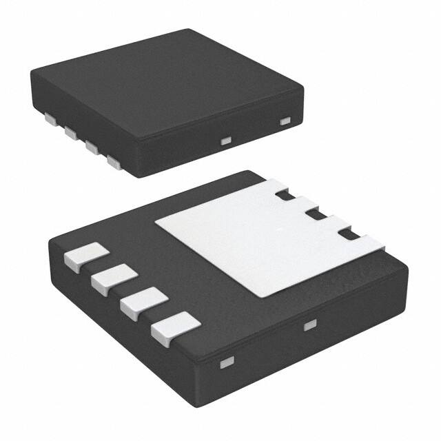
�FDMC010N08C
N-Channel Shielded Gate PowerTrench® MOSFET
80 V, 51 A, 10 mΩ
Features
General Description
Shielded Gate MOSFET Technology
This N-Channel MV MOSFET is produced using ON
Semiconductor’s advanced PowerTrench® process that
incorporates Shielded Gate technology. This process has been
optimized to minimise on-state resistance and yet maintain
superior switching performance with best in class soft body
diode.
Max rDS(on) = 10 mΩ at VGS = 10 V, ID = 16 A
Max rDS(on) = 25 mΩ at VGS = 6 V, ID = 8 A
50% lower Qrr than other MOSFET suppliers
Lowers switching noise/EMI
Applications
MSL1 robust package design
100% UIL tested
Primary DC-DC MOSFET
RoHS Compliant
Synchronous Rectifier in DC-DC and AC-DC
Motor Drive
Solar
Pin 1
Pin 1
S
D
Top
D
Power 33
D
S
S
S
D
S
D
S
D
G
D
G
D
Bottom
MOSFET Maximum Ratings TA = 25 °C unless otherwise noted
Symbol
VDS
Drain to Source Voltage
Parameter
VGS
Gate to Source Voltage
Drain Current -Continuous
ID
TC = 25 °C
-Continuous
TC = 100 °C
-Continuous
TA = 25 °C
-Pulsed
Single Pulse Avalanche Energy
EAS
PD
TJ, TSTG
TC = 25 °C
Power Dissipation
TA = 25 °C
Units
V
±20
V
(Note 5)
51
(Note 5)
32
(Note 1a)
11
(Note 4)
206
(Note 3)
Power Dissipation
Ratings
80
96
52
(Note 1a)
Operating and Storage Junction Temperature Range
2.4
-55 to +150
A
mJ
W
°C
Thermal Characteristics
RθJC
Thermal Resistance, Junction to Case
RθJA
Thermal Resistance, Junction to Ambient
2.4
(Note 1a)
53
°C/W
Package Marking and Ordering Information
Device Marking
FDMC010N08C
Device
FDMC010N08C
Package
Power 33
Semiconductor Components Industries, LLC, 2017
August, 2017, Rev. 1.0
Reel Size
13 ’’
Tape Width
12 mm
Quantity
3000 units
Publication Order Number:
FDMC010N08C/D
1
FDMC010N08C N-Channel Shielded Gate PowerTrench® MOSFET
www.onsemi.com
�Symbol
Parameter
Test Conditions
Min
Typ
Max
Units
Off Characteristics
BVDSS
Drain to Source Breakdown Voltage
ID = 250 μA, VGS = 0 V
ΔBVDSS
ΔTJ
Breakdown Voltage Temperature
Coefficient
ID = 250 μA, referenced to 25 °C
IDSS
Zero Gate Voltage Drain Current
VDS = 64 V, VGS = 0 V
1
μA
IGSS
Gate to Source Leakage Current
VGS = ±20 V, VDS = 0 V
±100
nA
4.0
V
80
V
75
mV/°C
On Characteristics
VGS(th)
Gate to Source Threshold Voltage
VGS = VDS, ID = 90 μA
ΔVGS(th)
ΔTJ
Gate to Source Threshold Voltage
Temperature Coefficient
ID = 90 μA, referenced to 25 °C
VGS = 10 V, ID = 16 A
8.0
10
rDS(on)
Static Drain to Source On Resistance
VGS = 6 V, ID = 8 A
12.3
25
VGS = 10 V, ID = 16 A, TJ = 125 °C
14
18
VDS = 5 V, ID = 16 A
35
gFS
Forward Transconductance
2.0
2.9
-8
mV/°C
mΩ
S
Dynamic Characteristics
Ciss
Input Capacitance
Coss
Output Capacitance
Crss
Reverse Transfer Capacitance
Rg
Gate Resistance
VDS = 40 V, VGS = 0 V,
f = 1 MHz
0.1
1070
1500
381
530
pF
pF
20
30
pF
0.4
0.7
Ω
Switching Characteristics
td(on)
Turn-On Delay Time
9
19
ns
tr
Rise Time
3
10
ns
td(off)
Turn-Off Delay Time
17
31
ns
tf
Fall Time
5
10
ns
nC
VDD = 40 V, ID = 16 A,
VGS = 10 V, RGEN = 6 Ω
Qg
Total Gate Charge
VGS = 0 V to 10 V
15
22
Qg
Total Gate Charge
VGS = 0 V to 6 V
10
14
Qgs
Gate to Source Charge
Qgd
Gate to Drain “Miller” Charge
Qoss
Output Charge
VDD = 40 V, VGS = 0 V
Qsync
Total Gate Charge Sync
VDS = 0 V, ID = 16 A
13.3
nC
VDD = 40 V,
ID = 16 A
nC
5
nC
3
nC
22.1
nC
Drain-Source Diode Characteristics
VSD
Source to Drain Diode Forward Voltage
trr
Reverse Recovery Time
Qrr
Reverse Recovery Charge
trr
Reverse Recovery Time
Qrr
Reverse Recovery Charge
VGS = 0 V, IS = 2 A
(Note 2)
0.7
1.2
VGS = 0 V, IS = 16 A
(Note 2)
0.8
1.3
IF = 8 A, di/dt = 300 A/μs
IF = 8 A, di/dt = 1000 A/μs
V
17
30
ns
20
33
nC
13
23
ns
45
73
nC
Notes:
1. RθJA is determined with the device mounted on a 1 in2 pad 2 oz copper pad on a 1.5 x 1.5 in. board of FR-4 material. RθCA is determined by the user's board design.
a. 53 °C/W when mounted on
a 1 in2 pad of 2 oz copper
b. 125 °C/W when mounted
on a minimum pad of 2 oz
copper
SS
SF
DS
DF
G
SS
SF
DS
DF
G
2. Pulse Test: Pulse Width < 300 μs, Duty cycle < 2.0%.
3. EAS of 96 mJ is based on starting TJ = 25 °C, L = 3 mH, IAS = 8 A, VDD = 72 V, VGS = 10 V, 100% test at L = 0.1 mH, IAS = 25 A.
4. Pulsed Id please refer to Fig 11 SOA graph for more details.
5. Computed continuous current limited to Max Junction Temperature only, actual continuous current will be limited by thermal & electro-mechanical application board design.
www.onsemi.com
2
FDMC010N08C N-Channel Shielded Gate PowerTrench® MOSFET
Electrical Characteristics TJ = 25 °C unless otherwise noted
�VGS = 10 V
VGS = 8 V
120
PULSE DURATION = 80 μs
VGS = 7 V DUTY CYCLE = 0.5% MAX
90
60
VGS = 6 V
30
VGS = 5.5 V
VGS = 5 V
0
0
1
2
3
4
5
NORMALIZED
DRAIN TO SOURCE ON-RESISTANCE
ID, DRAIN CURRENT (A)
150
VGS = 5 V
VGS = 5.5 V
4
VGS = 6 V
3
VGS = 7 V
VGS = 8 V
2
VGS = 10 V
1
PULSE DURATION = 80 μs
DUTY CYCLE = 0.5% MAX
0
5
0
30
VDS, DRAIN TO SOURCE VOLTAGE (V)
Figure 1. On Region Characteristics
rDS(on), DRAIN TO
1.6
1.4
1.2
1.0
0.8
0.6
-75
-50
-25
0
25
50
75
SOURCE ON-RESISTANCE (mΩ)
NORMALIZED
DRAIN TO SOURCE ON-RESISTANCE
80
ID = 16 A
VGS = 10 V
1.8
100 125 150
40
TJ = 125 oC
20
TJ = 25 oC
4
IS, REVERSE DRAIN CURRENT (A)
60
TJ = 150 oC
TJ = 25
oC
TJ = -55 oC
2
3
4
5
6
7
8
6
7
8
9
10
Figure 4. On-Resistance vs. Gate to
Source Voltage
90
30
5
VGS, GATE TO SOURCE VOLTAGE (V)
PULSE DURATION = 80 μs
DUTY CYCLE = 0.5% MAX
VDS = 5 V
120
150
ID = 16 A
60
0
Figure 3. Normalized On Resistance
vs. Junction Temperature
150
120
PULSE DURATION = 80 μs
DUTY CYCLE = 0.5% MAX
TJ, JUNCTION TEMPERATURE (oC)
ID, DRAIN CURRENT (A)
90
Figure 2. Normalized On-Resistance
vs. Drain Current and Gate Voltage
2.0
0
60
ID, DRAIN CURRENT (A)
9
150
100
VGS = 0 V
10
TJ = 150 oC
1
TJ = 25 oC
0.1
TJ = -55 oC
0.01
0.001
0.0
10
0.2
0.4
0.6
0.8
1.0
VGS, GATE TO SOURCE VOLTAGE (V)
VSD, BODY DIODE FORWARD VOLTAGE (V)
Figure 5. Transfer Characteristics
Figure 6. Source to Drain Diode
Forward Voltage vs. Source Current
www.onsemi.com
3
1.2
FDMC010N08C N-Channel Shielded Gate PowerTrench® MOSFET
Typical Characteristics TJ = 25 °C unless otherwise noted.
�10000
ID = 16 A
VDD = 30 V
8
Ciss
CAPACITANCE (pF)
VGS, GATE TO SOURCE VOLTAGE (V)
10
VDD = 40 V
6
VDD = 50 V
4
1000
Coss
100
Crss
10
2
0
f = 1 MHz
VGS = 0 V
0
3
6
9
12
15
1
0.1
18
1
10
80
VDS, DRAIN TO SOURCE VOLTAGE (V)
Qg, GATE CHARGE (nC)
Figure 7. Gate Charge Characteristics
Figure 8. Capacitance vs. Drain
to Source Voltage
100
60
ID, DRAIN CURRENT (A)
IAS, AVALANCHE CURRENT (A)
o
TJ = 25 oC
10
TJ = 100 oC
TJ = 125 oC
1
0.001
0.01
0.1
RθJC = 2.4 C/W
50
40
VGS = 10 V
30
20
VGS = 6 V
10
1
10
0
25
100
50
100
125
150
TC, CASE TEMPERATURE ( C)
Figure 9. Unclamped Inductive
Switching Capability
Figure 10. Maximum Continuous Drain
Current vs. Case Temperature
300
P(PK), PEAK TRANSIENT POWER (W)
10000
100
ID, DRAIN CURRENT (A)
75
o
tAV, TIME IN AVALANCHE (ms)
10 μs
SINGLE PULSE
RθJC = 2.4 oC/W
TC = 25 oC
1000
10
THIS AREA IS
LIMITED BY rDS(on)
1
SINGLE PULSE
TJ = MAX RATED
RθJC = 2.4 oC/W
TC = 25 oC
0.1
0.1
100 μs
1
1 ms
CURVE BENT TO
MEASURED DATA
10
10 ms
100 ms/DC
100
500
100
10
-5
10
-4
10
-3
10
-2
10
-1
10
t, PULSE WIDTH (sec)
VDS, DRAIN to SOURCE VOLTAGE (V)
Figure 11. Forward Bias Safe
Operating Area
Figure 12. Single Pulse Maximum
Power Dissipation
www.onsemi.com
4
1
FDMC010N08C N-Channel Shielded Gate PowerTrench® MOSFET
Typical Characteristics TJ = 25 °C unless otherwise noted.
�r(t), NORMALIZED EFFECTIVE TRANSIENT
THERMAL RESISTANCE
2
1
0.1
DUTY CYCLE-DESCENDING ORDER
D = 0.5
0.2
0.1
0.05
0.02
0.01
PDM
t1
t2
0.01
0.001
-5
10
SINGLE PULSE
NOTES:
ZθJC(t) = r(t) x RθJC
RθJC = 2.4 oC/W
Peak TJ = PDM x ZθJC(t) + TC
Duty Cycle, D = t1 / t2
-4
10
-3
-2
10
10
Figure 13. Junction-to-Case Transient Thermal Response Curve
www.onsemi.com
5
-1
10
t, RECTANGULAR PULSE DURATION (sec)
1
FDMC010N08C N-Channel Shielded Gate PowerTrench® MOSFET
Typical Characteristics TJ = 25 °C unless otherwise noted.
�FDMC010N08C N-Channel Shielded Gate PowerTrench® MOSFET
Dimensional Outline and Pad Layout
ON Semiconductor and the ON Logo are trademarks of Semiconductor Components Industries, LLC dba ON Semiconductor or its subsidiaries in the United States and/or other
countries.
ON Semiconductor owns the rights to a number of patents, trademarks, copyrights, trade secrets, and other intellectual property. A listing of ON Semiconductor's product/patent
coverage may be accessed at www.onsemi.com/site/pdf/Patent-Marking.pdf. ON Semiconductor reserves the right to make changes without further notice to any products herein.
ON Semiconductor makes no warranty, representation or guarantee regarding the suitability of its products for any particular purpose, nor does ON Semiconductor assume any
liability arising out of the application or use of any product or circuit, and specifically disclaims any and all liability, including without limitation special, consequential or incidental
damages. Buyer is responsible for its products and applications using ON Semiconductor products, including compliance with all laws, regulations and safety requirements or
standards, regardless of any support or applications information provided by
ON Semiconductor. “Typical” parameters which may be provided in ON Semiconductor data sheets and/or specifications can and do vary in different applications and actual
performance may vary over time. All operating parameters, including “Typicals” must be validated for each customer application by customer's technical experts. ON
Semiconductor does not convey any license under its patent rights nor the rights of others. ON Semiconductor products are not designed, intended, or authorized for use as a
critical component in life support systems or any FDA Class 3 medical devices or medical devices with a same or similar classification in a foreign jurisdiction or any devices
intended for implantation in the human body. Should Buyer purchase or use ON Semiconductor products for any such unintended or unauthorized application, Buyer shall
indemnify and hold ON Semiconductor and its officers, employees, subsidiaries, affiliates, and distributors harmless against all claims, costs, damages, and expenses, and
reasonable attorney fees arising out of, directly or indirectly, any claim of personal injury or death associated with such unintended or unauthorized use, even if such claim alleges
that ON Semiconductor was negligent regarding the design or manufacture of the part. ON Semiconductor is an Equal Opportunity/Affirmative Action Employer. This literature is
subject to all applicable copyright laws and is not for resale in any manner.
www.onsemi.com
6
�


 工商网监
湘ICP备2023018690号
工商网监
湘ICP备2023018690号
