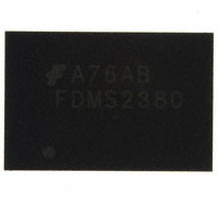
FDMS2380
Dual Integrated Solenoid Driver
Features
General Description
5A, 60V Load Clamp
The FDMS2380 is an intelligent low side driver with built in
recirculation and demagnetization circuits designed
specifically for driving inductive loads. The inputs are
CMOS compatible. A separate diagnostic signal for each
channel provides the system with an indication of the
operation of the solenoid or the presence of a protection
fault condition. Built-in Over-voltage, Over-current, Overtemperature circuits protect the device from these
conditions. Additional diagnostic circuitry is included for
detecting Open Load, Under-voltage and output ground
fault conditions. The FDMS2380 contains two independent
intelligent low side solenoid drivers.
rDS(ON) = 30mΩ (Typ.) Excitation path
6V to 26V Operation
CMOS Compatible
Soft Short Detection
Thermal Shutdown
Diagnostic Output
Integrated Clamps
Over-current Protection
Open Load Detection
Over-voltage Protection
Pin 1
Applications
Transmission Solenoid Driver
Inductive Load Management
Power QFN
Internal Logical Block Diagram (One of two Identical Channels)
VBATT
Volt Regulator
& Over / Under
Voltage Detect
Soft Short
&
Recirculation
PDMOS
Driver
& Clamp
Power
PDMOS
Recirculation
Device
Over Temp
Shutdown
INA
Control
Logic
INB
OUT
Open Load
Detect
Power
NDMOS
DIAG
Diagnostic Control
&
Pulse Generation
Over
Current
Shutdown
NDMOS
Driver
Excitation
Device
GND
©2007 Fairchild Semiconductor Corporation
FDMS2380 Rev. A
1
www.fairchildsemi.com
FDMS2380 Dual Integrated Solenoid Driver
August 2007
�FDMS2380 Dual Integrated Solenoid Driver
Pin Assignment
OUT2
GND2
1
2
OUT2
3
VBATT
4
OUT1
5
DIAG1
6
INB1
7
INA1
8
OUT1
9
OUT2
VBATT
OUT1
18
OUT2
17
INA2
16
INB2
15
DIAG2
14
OUT2
13
VBATT
12
OUT1
11
GND1
10
OUT1
TOP VIEW
Pin Description
QFN Pin
Pin Name
1, 3, 14, 18, pad OUT2
OUT2
Power Driver Output (Ch2)
Pin Description
2
GND2
Ground (Ch2)
4, 13, pad VBATT
VBATT
Battery Supply Voltage. Battery supply is common to both channels
5, 9, 10, 12, pad OUT1
OUT1
Power Driver Output (Ch1)
6
DIAG1
Diagnostic Flag (Ch1). Open drain output.
7
INB1
8
INA1
Input Control Signal A (Ch1)
11
GND1
Ground (Ch1)
15
DIAG2
16
INB2
Input Control Signal B (Ch2)
17
INA2
Input Control Signal A (Ch2)
Input Control Signal B (Ch1)
Diagnostic Flag (Ch2). Open drain output.
2
FDMS2380 Rev. A
www.fairchildsemi.com
�Symbol
Parameter
Ratings
Units
-4
A
IOUT(rev)
Maximum Reverse Output Current
VBATT(max)
Maximum DC Supply Voltage (Note 2)
60
V
IIN
Input Currents
10
mA
VIN(max)
Maximum Input Voltage
8
V
IDIAG
Diagnostic Output Current
10
mA
VDIAG(max)
Maximum Diagnostic Output Voltage
8
V
Total Power dissipation
PD
TJ, TSTG
7
W
Power dissipation VBATT pad
2.3
W
Power dissipation OUT pads: PD(OUT) = PD(OUT1) + PD(OUT2)
4.6
W
-40 to 160
oC
Operating and Storage Temperature
Thermal Characteristics
RθJC
Thermal Resistance Junction to Case: OUT pad
3.5
oC/W
RθJC
Thermal Resistance Junction to Case: VBATT pad
4.0
oC/W
RθJA
Thermal Resistance Junction to Ambient: OUT pad (Note 1)
60
oC/W
RθJA
Thermal Resistance Junction to Ambient: VBATT pad (Note 1)
60
oC/W
Ordering Information
Part Number
Package
Packing
Method
Reel Size
Tape Width
Quantity
FDMS2380
18 pin QFN
Tape & Reel
330mm
24mm
2000
Notes:
1. RθJA is measured with 1.0 in2 copper on FR-4 board. RθJC is guaranteed by design while RθJA is determined by the user’s board design.
2. The FDMS2380 requires one or more high quality local bypass capacitors (i.e., low ESL, low ESR and located physically close to the VBATT/Ground terminals of
the device) to prevent fast transients on the VBATT line from affecting the operation of the device. More specifically, the bypass scheme must reduce transients
with an amplitude passing through VBATT(ov) to have a rise time of less than 2.2V/µs.
3
FDMS2380 Rev. A
www.fairchildsemi.com
FDMS2380 Dual Integrated Solenoid Driver
Maximum Ratings TC = 25°C unless otherwise noted
�Symbol
Parameter
Test Conditions
Min
Typ
Max
Units
---
6.0
14.0
26.0
V
Off Characteristics
VBATT(Oper) Operating Supply Voltage
ISQ
Supply Quiescent Current
VBATT = 13V, VINA = VINB = 5V
-
9.3
15
mA
ILK
Output Leakage Current
VBATT = 18V, VINA = VINB = 1.5V
-
0.2
5
mA
On Characteristics
rDS(ON)
On Resistance - Excitation Path
VRecir(sat)
Saturation Voltage - Recirculation
Path
VBATT = 13V, VINA = VINB = 5V,
-
0.030
0.080
Ω
IOUT = 5A
-
0.050
0.100
Ω
-
1.4
1.8
V
TC = 150oC
VBATT = 13V, VINA = 5V,
VINB = 0V, IOUT = 10A
Switching Characteristics (Excitation Path)
td(ON)
Output Turn-On Delay Time
-
7.0
30
μs
td(OFF)
Output Turn-Off Delay Time
-
8.3
30
μs
tr
Rise Time
-
6.5
10
μs
tf
Fall Time
-
3.0
10
μs
VBATT = 14V, RLoad = 2.5Ω
Logic Input Characteristics
VIL
Input Low Level Voltage
---
-
-
1.5
V
VIH
Input High Level Voltage
---
3.5
-
-
V
VCL
Input Clamp Voltage
IIN
Input Current (each input)
IIN
很抱歉,暂时无法提供与“FDMS2380”相匹配的价格&库存,您可以联系我们找货
免费人工找货- 国内价格
- 1+141.56640
- 200+54.78840
- 500+52.86600
- 1000+51.90480
