DATA SHEET
www.onsemi.cn
MOSFET – N 沟道,
POWERTRENCH)
VDSS
RDS(ON) MAX
ID MAX
150 V
7.5 mW @ 10 V
130 A
*������� 120 A。
150 V, 130 A, 7.5 mW
FDP075N15A, FDB075N15A
说�
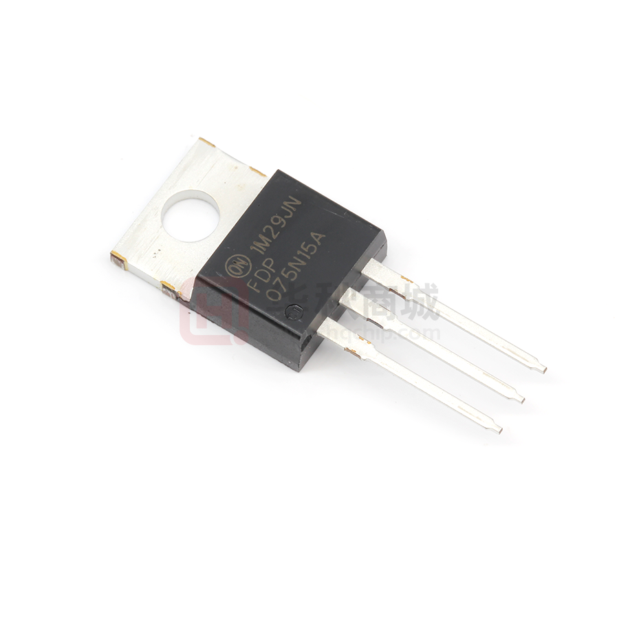
TO−220
CASE 221A−09
� N � � MOSFET � � onsemi � � POWERTRENCH
����, ������
��
�����
���
�����������。
G
特�
D
S
D
•�RDS(on) = 6.25 mW (���) @ VGS = 10 V, ID = 100 A
•�����
•�� !
�
•������"#$%�!�� RDS(on)
•��&�'�
()��*
•��+ RoHS ,-
G
D2PAK−3 (TO−263, 3−LEAD)
CASE 418AJ
S
MARKING DIAGRAM
�用
•��. ATX / /01 /
2 PSU �345(
•�
6�7
�
•�
8�9':�;
<
•�=�>���?1
$Y&Z&3&K
FDB
075N15A
$Y&Z&3&K
FDP
075N15A
$Y
FDP075N15A
FDB075N15A
&Z
&3
&K
= onsemi logo
= Device Code
= Assembly Plant Code
= 3−Digit Date Code Format
= 2−Digits Lot Run Traceability Code
D
G
S
N−Channel
ORDERING INFORMATION
See detailed ordering and shipping information on page 9 of
this data sheet.
© Semiconductor Components Industries, LLC, 2017
September, 2021 − Rev. 3
1
Publication Order Number:
FDP075N15ACN/D
�FDP075N15A, FDB075N15A
MOSFET 最�额�� (TC = 25°C ���
�。)
符�
FDP075N15A−F102
FDB075N15A
��
VDSS
�
-�
��
150
V
VGSS
�
-�
��
±20
V
- �� (TC = 25°C)
130*
A
- �� (TC = 100°C)
92
- �� (
� 1)
522
A
ID
�
��
IDM
�
��
EAS
������� (
� 2)
588
mJ
dv/dt
��
dv/dt �� (
� 3)
6.0
V/ns
(TC = 25°C)
333
W
- �
� 25°C ��
2.22
W/°C
-55 � +175
°C
300
°C
PD
TJ, TSTG
TL
��
������
!�
"�#$%&�'(�
,*+�� 1/8”,,� 5 -
Stresses exceeding those listed in the Maximum Ratings table may damage the device. If any of these limits are exceeded, device functionality
should not be assumed, damage may occur and reliability may be affected.
(�./0)
�1��23&�45�6���%�!�,�� �!7"。�123#$8%��,9:;&��7",?'
@A。
*������� 120 A。
1. B
45�:��D (��&�E�。
2. F) TJ = 25°C, L = 3 mH, IAS = 19.8 A。
3. ISD ≤ 100 A, di/dt ≤ 200 A/ms, VDD ≤ BVDSS, F) TJ = 25°C.
热�能
符�
RqJC
E���GH&��
RqJA
E�I+GH (&JKL% 2 M,#N) &��。
E�I+GH D2-PAK (1
in2
FDP075N15A−F102
FDB075N15A
��
0.45
°C/W
62.5
40
2 M,#N) &��。
www.onsemi.cn
2
�FDP075N15A, FDB075N15A
ELECTRICAL CHARACTERISTICS (TC = 25°C unless otherwise noted)
符�
测试条
最��
���
最��
��
150
−
−
V
−
0.1
−
V/°C
VDS = 120 V, VGS = 0 V
−
−
1
mA
��特�
BVDSS
DBVDSS /
DTJ
�
-�
/O��
ID = 250 mA, VGS = 0 V
/O���
ID = 250 mA, �
PQ
�. 25°C
IDSS
R�
���
��
VDS = 120 V, TC = 150°C
−
−
500
IGSS
�
-0���
VGS = ±20 V, VDS = 0 V
−
−
±100
nA
VGS(th)
�
S���
VGS = VDS, ID = 250 mA
2.0
−
4.0
V
RDS(on)
�
��
TU=V�H
VGS = 10 V, ID = 100 A
−
6.25
7.5
mW
W4X=
VDS = 10 V, ID = 100 A
−
164
−
S
Ciss
Y5�Z
VDS = 75 V, VGS = 0 V, f = 1 MHz
−
5525
7350
pF
Coss
Y��Z
−
516
685
pF
Crss
647Y�Z
−
21
−
pF
�通特�
gFS
��特�
Coss(er)
��[8Y��Z
VDS = 75 V, VGS = 0 V
−
909
−
pF
Qg(tot)
10 V %�
�\]�
VDS = 75 V, ID = 100 A, VGS = 10 V
(
� 4)
−
77
100
nC
Qgs
�
- �
�
�\
−
26
−
nC
Qgs2
�
^:�\S�
−
11
−
nC
Qgd
�
- �
“_;” �\
−
16
−
nC
ESR
`a�ef
−
21
52
ns
漏极 - 源极�极管特�
IS
�
- �
�&�W4����
−
−
130*
A
ISM
�
- �
�&�W4����
−
−
520
A
VSD
�
- �
�W4��
VGS = 0 V, ISD = 100 A
−
−
1.25
V
trr
64�
ef
−
97
−
ns
Qrr
64�
�\
VGS = 0 V, VDD = 75 V, ISD = 100 A,
dIF/dt = 100 A/ms
−
264
−
nC
4. hi�jk����
%?@lA。
www.onsemi.cn
3
�FDP075N15A, FDB075N15A
���能特�
400
VGS =15.0 V
10.0 V
8.0 V
7.0 V
6.5 V
100
6.0 V
5.5 V
5.0 V
ID, Drain Current (A)
ID, Drain Current (A)
400
*Notes:
1. 250 ms Pulse Test
2. TC = 25°C
10
7
0.1
1
100
175°C
25°C
VDS, Drain−Source Voltage (V)
IS, Reverse Drain Current (A)
RDS(ON), Drain−Source On−Resistance (mW)
5
6
400
8
VGS = 10 V
VGS = 20 V
6
*Note: TC = 25°C
100
200
300
100
175°C
25°C
10
1
0.0
400
ID, Drain Current (A)
*Notes:
1. VGS = 0 V
2. 250 ms Pulse Test
0.5
1.0
1.5
VSD, Body Diode Forward Voltage (V)
图 3. �通电阻���漏极电流�栅极电!
图 4. "�极管正#电!���源极电流�温$
10000
10
1000
VGS, Gate−Source Voltage (V)
Ciss
Capacitance (pF)
4
图 2. �输特�
10
Coss
*Notes:
100 1. VGS = 0 V
2. f = 1 MHz
10
0.1
3
VGS, Gate−Source Voltage (V)
图 1. �通��特�
4
0
−55°C
10
1
2
3
*Notes:
1. VDS = 10 V
2. 250 ms Pulse Test
Ciss = Cgs + Cgd (Cds = shorted)
Coss = Cds + Cgd
Crss = Cgd
1
Crss
10
8
6
4
2
0
0
100 200
VDS, Drain−Source Voltage (V)
VDS = 30 V
VDS = 75 V
VDS = 120 V
*Note: ID = 100 A
30
60
Qg, Total Gate Charge (nC)
图 5. 电%特�
图 6. 栅极电荷
www.onsemi.cn
4
90
�FDP075N15A, FDB075N15A
1.10
RDS(ON), Drain−Source On−Resistance
(Normalized)
BVDSS, Drain−Source Breakdown Voltage
(Normalized)
���能特� ($�m)
1.05
1.00
0.95
0.90
−100
*Notes:
1. VGS = 0 V
2. ID = 250 mA
−50
0
50
100
150
200
3.0
2.5
2.0
1.5
1.0
0.0
−100
TJ, Junction Temperature (°C)
ID, Drain Current (A)
ID, Drain Current (A)
150
200
1 ms
10
10 ms
100 ms
Operation in This Area
is Limited by RDS(on)
*Notes:
1. TC = 25°C
2. TJ = 175°C
3. Single Pulse
VGS = 10 V
DC
100
Limited by package
80
60
40
20
1
10
100
RqJC = 0.45°C/W
0
25
300
50
VDS, Drain−Source Voltage (V)
50
IAS, Avalanche Current (A)
5
4
3
2
1
75
100
125
150
175
If R = 0
tAV = (L)(IAS)/(1.3*Rated BVDSS−VDD)
If R = 0
tAV = (L/R)In[(IAS*R)/(1.3*Rated BVDSS−VDD)+1]
6
50
100
图 10. 最�漏极电流�+,温$
7
25
75
TC, Case Temperature (°C)
图 9. 最�'()*�
EOSS (mJ)
100
120
100
0
0
50
140
100 ms
0.01
0.1
0
图 8. �通电阻���温$
1000
0.1
−50
TJ, Junction Temperature (°C)
图 7. &穿电!���温$
1
*Notes:
1. VGS = 10 V
2. ID = 100 A
0.5
125
Starting TJ = 25°C
10
Starting TJ = 150°C
1
0.01
150
VDS, Drain to Source Voltage (V)
0.1
1
10
100
TAV, Time in Avalanche (ms)
图 11. 输/电% (Eoss) �漏极 - 源极电
图 12. 非箝�电:��能;
www.onsemi.cn
5
500
�FDP075N15A, FDB075N15A
���能特� ($�m)
ZqJC(t), G'n (°C/W)
1
0.1
PDM
t1
t2
*Notes:
1. ZqJC(t) = 0.45°C/W Max.
2. Duty Factor, D= t1 / t2
3. TJM − TC = PDM * ZqJC(t)
0.01
0.001
−5
10
−4
10
−3
10
−2
10
t1, op��,�ef (-)
图 13. 瞬�热
V DS
RG
VGS
10V
RL
V DS
90%
V DD
V GS
V GS
DUT
10%
tr
td(on)
t on
图 15. 阻���测试电路�波>
VGS
图 16. 非箝�电:��测试电路�波>
www.onsemi.cn
7
td(off)f)
t off
tf
�FDP075N15A, FDB075N15A
DUT
+
V DS
_
ISD
L
Driver
RG
Same Type
as DUT
V GS
V GS
(Driver)
V DD
• dv/dt controlled by RG
• ISD controlled by pulse period
D=
Gate Pulse Width
Gate Pulse Period
10 V
I FM , Body Diode Forward Current
I SD
di/dt
(DUT)
I RM
Body Diode Reverse Current
V DS
(DUT)
Body Diode Recovery dv/dt
V SD
Body Diode
Forward Voltage Drop
图 17. �极管?@ dv/dt A�测试电路�波>
www.onsemi.cn
8
V DD
�FDP075N15A, FDB075N15A
B装标识��购CD
E
编�
顶标
B装
F装G法†
HIJ
KL
量
FDP075N15A−F102
FDP075N15A
TO−220
Ar�
Bs"
Bs"
50 C
FDB075N15A
FDB075N15A
D2−PAK
Dt
330 mm
24 mm
800 C
†For information on tape and reel specifications, including part orientation and tape sizes, please refer to our Tape and Reel Packaging
Specifications Brochure, BRD8011/D.
POWERTRENCH is registered trademark of Semiconductor Components Industries, LLC dba “onsemi” or its affiliates and/or subsidiaries in the United
States and/or other countries.
www.onsemi.cn
9
�MECHANICAL CASE OUTLINE
PACKAGE DIMENSIONS
TO−220
CASE 221A−09
ISSUE AJ
DATE 05 NOV 2019
SCALE 1:1
STYLE 1:
PIN 1.
2.
3.
4.
BASE
COLLECTOR
EMITTER
COLLECTOR
STYLE 2:
PIN 1.
2.
3.
4.
BASE
EMITTER
COLLECTOR
EMITTER
STYLE 3:
PIN 1.
2.
3.
4.
CATHODE
ANODE
GATE
ANODE
STYLE 4:
PIN 1.
2.
3.
4.
MAIN TERMINAL 1
MAIN TERMINAL 2
GATE
MAIN TERMINAL 2
STYLE 5:
PIN 1.
2.
3.
4.
GATE
DRAIN
SOURCE
DRAIN
STYLE 6:
PIN 1.
2.
3.
4.
ANODE
CATHODE
ANODE
CATHODE
STYLE 7:
PIN 1.
2.
3.
4.
CATHODE
ANODE
CATHODE
ANODE
STYLE 8:
PIN 1.
2.
3.
4.
CATHODE
ANODE
EXTERNAL TRIP/DELAY
ANODE
STYLE 9:
PIN 1.
2.
3.
4.
GATE
COLLECTOR
EMITTER
COLLECTOR
STYLE 10:
PIN 1.
2.
3.
4.
GATE
SOURCE
DRAIN
SOURCE
STYLE 11:
PIN 1.
2.
3.
4.
DRAIN
SOURCE
GATE
SOURCE
STYLE 12:
PIN 1.
2.
3.
4.
MAIN TERMINAL 1
MAIN TERMINAL 2
GATE
NOT CONNECTED
DOCUMENT NUMBER:
DESCRIPTION:
98ASB42148B
TO−220
Electronic versions are uncontrolled except when accessed directly from the Document Repository.
Printed versions are uncontrolled except when stamped “CONTROLLED COPY” in red.
PAGE 1 OF 1
ON Semiconductor and
are trademarks of Semiconductor Components Industries, LLC dba ON Semiconductor or its subsidiaries in the United States and/or other countries.
ON Semiconductor reserves the right to make changes without further notice to any products herein. ON Semiconductor makes no warranty, representation or guarantee regarding
the suitability of its products for any particular purpose, nor does ON Semiconductor assume any liability arising out of the application or use of any product or circuit, and specifically
disclaims any and all liability, including without limitation special, consequential or incidental damages. ON Semiconductor does not convey any license under its patent rights nor the
rights of others.
© Semiconductor Components Industries, LLC, 2019
www.onsemi.com
�MECHANICAL CASE OUTLINE
PACKAGE DIMENSIONS
D2PAK−3 (TO−263, 3−LEAD)
CASE 418AJ
ISSUE F
SCALE 1:1
GENERIC MARKING DIAGRAMS*
XX
XXXXXXXXX
AWLYWWG
IC
DOCUMENT NUMBER:
DESCRIPTION:
XXXXXXXXG
AYWW
Standard
98AON56370E
AYWW
XXXXXXXXG
AKA
Rectifier
XXXXXX
XXYMW
SSG
DATE 11 MAR 2021
XXXXXX = Specific Device Code
A
= Assembly Location
WL
= Wafer Lot
Y
= Year
WW
= Work Week
W
= Week Code (SSG)
M
= Month Code (SSG)
G
= Pb−Free Package
AKA
= Polarity Indicator
*This information is generic. Please refer to
device data sheet for actual part marking.
Pb−Free indicator, “G” or microdot “ G”,
may or may not be present. Some products
may not follow the Generic Marking.
Electronic versions are uncontrolled except when accessed directly from the Document Repository.
Printed versions are uncontrolled except when stamped “CONTROLLED COPY” in red.
D2PAK−3 (TO−263, 3−LEAD)
PAGE 1 OF 1
ON Semiconductor and
are trademarks of Semiconductor Components Industries, LLC dba ON Semiconductor or its subsidiaries in the United States and/or other countries.
ON Semiconductor reserves the right to make changes without further notice to any products herein. ON Semiconductor makes no warranty, representation or guarantee regarding
the suitability of its products for any particular purpose, nor does ON Semiconductor assume any liability arising out of the application or use of any product or circuit, and specifically
disclaims any and all liability, including without limitation special, consequential or incidental damages. ON Semiconductor does not convey any license under its patent rights nor the
rights of others.
© Semiconductor Components Industries, LLC, 2018
www.onsemi.com
�onsemi,
, and other names, marks, and brands are registered and/or common law trademarks of Semiconductor Components Industries, LLC dba “onsemi” or its affiliates
and/or subsidiaries in the United States and/or other countries. onsemi owns the rights to a number of patents, trademarks, copyrights, trade secrets, and other intellectual property.
A listing of onsemi’s product/patent coverage may be accessed at www.onsemi.com/site/pdf/Patent−Marking.pdf. onsemi reserves the right to make changes at any time to any
products or information herein, without notice. The information herein is provided “as−is” and onsemi makes no warranty, representation or guarantee regarding the accuracy of the
information, product features, availability, functionality, or suitability of its products for any particular purpose, nor does onsemi assume any liability arising out of the application or use
of any product or circuit, and specifically disclaims any and all liability, including without limitation special, consequential or incidental damages. Buyer is responsible for its products
and applications using onsemi products, including compliance with all laws, regulations and safety requirements or standards, regardless of any support or applications information
provided by onsemi. “Typical” parameters which may be provided in onsemi data sheets and/or specifications can and do vary in different applications and actual performance may
vary over time. All operating parameters, including “Typicals” must be validated for each customer application by customer’s technical experts. onsemi does not convey any license
under any of its intellectual property rights nor the rights of others. onsemi products are not designed, intended, or authorized for use as a critical component in life support systems
or any FDA Class 3 medical devices or medical devices with a same or similar classification in a foreign jurisdiction or any devices intended for implantation in the human body. Should
Buyer purchase or use onsemi products for any such unintended or unauthorized application, Buyer shall indemnify and hold onsemi and its officers, employees, subsidiaries, affiliates,
and distributors harmless against all claims, costs, damages, and expenses, and reasonable attorney fees arising out of, directly or indirectly, any claim of personal injury or death
associated with such unintended or unauthorized use, even if such claim alleges that onsemi was negligent regarding the design or manufacture of the part. onsemi is an Equal
Opportunity/Affirmative Action Employer. This literature is subject to all applicable copyright laws and is not for resale in any manner.
PUBLICATION ORDERING INFORMATION
LITERATURE FULFILLMENT:
Email Requests to: orderlit@onsemi.com
onsemi Website: www.onsemi.com
◊
TECHNICAL SUPPORT
North American Technical Support:
Voice Mail: 1 800−282−9855 Toll Free USA/Canada
Phone: 011 421 33 790 2910
Europe, Middle East and Africa Technical Support:
Phone: 00421 33 790 2910
For additional information, please contact your local Sales Representative
�