FDP4020P/FDB4020P
P-Channel 2.5V Specified Enhancement Mode Field Effect Transistor
General Description
Features
This P-Channel low threshold MOSFET has been
designed for use as a linear pass element for low voltage
outputs. In addition, the part may be used as a low voltage
load switch when switching outputs on or off for power
management.The part may also be used in conjunction
with DC-DC converters requiring P-Channel.
• -16 A, -20 V. RDS(on) = 0.08 Ω @ VGS = -4.5 V
RDS(on) = 0.11 Ω @ VGS = -2.5 V.
• Critical DC electrical parameters specified at elevated
temperature.
• High density cell design for extremely low RDS(on).
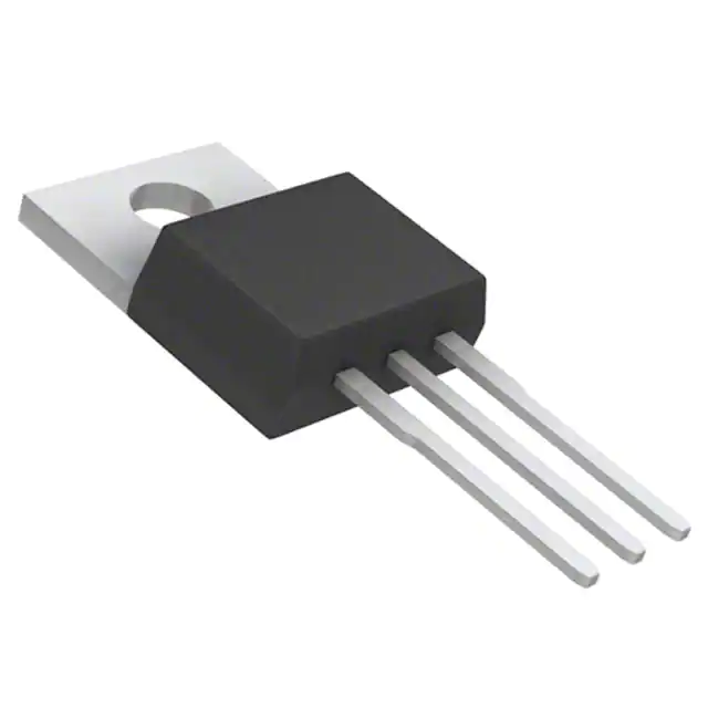
• TO-220 and TO-263 (D2PAK) package for both
through hole and surface mount applications.
• 175°C maximum junction temperature rating.
S
G
D
A bsolute M axim um Ratings
Sym bol
T A = 25°C unless otherw ise noted
FD P4020P
Param eter
FD B 4020P
U nits
V DSS
Drain-S ource V oltage
-20
V
V G SS
G ate-S ource V oltage
ID
Drain Current
±8
-16
A
PD
Total P ower Dissipation @ T C = 25 ° C
T J , T STG
Derate above 25 ° C
O perating and S torage Junction Tem perature Range
- Continuous
- P ulsed
V
-48
37.5
W
0.25
-65 to +175
W /° C
°C
Therm al C haracteristics
R θ JC
Therm al Resistance, Junction-to- Case
R θ JA
Therm al Resistance, Junction-to- A m bient
4
(N ote 1)
62.5
40
° C/W
° C/W
Package O utlines and O rdering Inform ation
D evice M arking
D evice
R eel Size
Tape W idth
Q uantity
FDP 4020P
FDP 4020P
13’’
12m m
2500 units
2000 Fairchild Semiconductor International
FDP4020P Rev. B
FDP4020P
September 2000
�Symbol
Parameter
TA = 25°C unless otherwise noted
Test Conditions
Min
Typ
Max
Units
Off Characteristics
BVDSS
∆BVDSS
∆T J
IDSS
IGSSF
IGSSR
Drain-Source Breakdown
VGS = 0 V, ID = -250 µA
Voltage
Breakdown Voltage
ID = -250 µA, Referenced to 25°C
Temperature Coefficient
Zero Gate Voltage Drain Current VDS = -16 V, VGS = 0 V
Gate-Body Leakage Current,
Forward
Gate-Body Leakage Current,
Reverse
On Characteristics
-20
V
mV/°C
-28
VGS = 8 V, VDS = 0 V
100
µA
nA
VGS = -8 V, VDS = 0 V
-100
nA
-1
(Note 2)
VGS(th)
Gate Threshold Voltage
VDS = VGS, ID = -250 µA
∆VGS(th)
∆T J
RDS(on)
Gate Threshold Voltage
Temperature Coefficient
Static Drain-Source
On-Resistance
ID = -250 µA, Referenced to 25°C
ID(on)
On-State Drain Current
VGS = -4.5 V, VDS = -5 V
gFS
Forward Transconductance
VDS = -5 V, ID = -8 A
14
VDS = -10 V, VGS = 0 V,
f = 1.0 MHz
665
pF
270
pF
70
pF
-0.4
-0.58
-1
VGS = -4.5 V,ID = -8 A,
VGS = -4.5 V,ID = -8 A,TJ=125°C
VGS = -2.5 V,ID = -7 A
0.068
0.098
0.096
V
mV/°C
2
0.08
0.13
0.110
-20
Ω
A
S
Dynamic Characteristics
Ciss
Input Capacitance
Coss
Output Capacitance
Crss
Reverse Transfer Capacitance
Switching Characteristics
(Note 2)
VDD = -5 V, ID = -1 A,
VGS = -4.5 V, RGEN = 6 Ω
td(on)
Turn-On Delay Time
tr
Turn-On Rise Time
td(off)
Turn-Off Delay Time
50
80
ns
tf
Turn-Off Fall Time
29
45
ns
Qg
Total Gate Charge
9.5
13
nC
Qgs
Gate-Source Charge
Qgd
Gate-Drain Charge
VDS = -5 V,
ID = -16 A, VGS = -4.5 V
8
16
ns
24
38
ns
1.3
nC
2.2
nC
Drain-Source Diode Characteristics and Maximum Ratings
IS
Maximum Continuous Drain-Source Diode Forward Current
(Note 2)
-16
ISM
Maximum Pulsed Drain-Source Diode Forward Current
(Note 2)
-48
VSD
Drain-Source Diode Forward
Voltage
(Note 2)
-1.2
VGS = 0 V, IS = -16 A
A
V
Notes:
1. RθJA is the sum of the juntion-to-case and case-to-ambient thermal resistance.For T0-263 the device is mounted on circuit board with a 1in2 pad
of 2 oz. copper.
2. Pulse Test: Pulse Width ≤ 300 µs, Duty Cycle ≤ 2.0%
FDP4020P Rev. B
FDP4020P
Electrical Characteristics
�FDP4020P
Typical Characteristics
40
2
RDS(ON), NORMALIZED
DRAIN-SOURCE ON-RESISTANCE
-ID, DRAIN CURRENT (A)
VGS = -4.5V
-4.0V
32
-3.5V
-3.0V
24
16
-2.5V
8
-2.0V
0
1.8
VGS = -2.0V
1.6
-2.5V
1.4
-3.0V
1.2
-3.5V
-4.0V
0.8
0
2
4
6
8
10
0
5
10
-VDS, DRAIN-SOURCE VOLTAGE (V)
20
25
30
Figure 2. On-Resistance Variation
with Drain Current and Gate Voltage.
0.2
1.8
ID = -16A
VGS = -4.5V
1.6
RDS(ON), ON-RESISTANCE (OHM)
RDS(ON), NORMALIZED
DRAIN-SOURCE ON-RESISTANCE
15
-ID, DIRAIN CURRENT (A)
Figure 1. On-Region Characteristics.
1.4
1.2
1
0.8
ID = -8A
0.16
0.12
o
TA = 125 C
0.08
o
TA = 25 C
0.04
0
0.6
-50
-25
0
25
50
75
100
125
150
1.5
175
2
2.5
3
3.5
4
4.5
5
-VGS, GATE TO SOURCE VOLTAGE (V)
o
TJ, JUNCTION TEMPERATURE ( C)
Figure 3. On-Resistance Variation
with Temperature.
Figure 4. On-Resistance Variation
with Gate-to-Source Voltage.
20
100
TA = -55 C
-IS, REVERSE DRAIN CURRENT (A)
o
VDS = -5V
-ID, DRAIN CURRENT (A)
-4.5V
1
o
25 C
o
16
125 C
12
8
4
VGS = 0V
1
o
TA = 125 C
o
25 C
o
-55 C
0.01
0.0001
0
0
0.5
1
1.5
2
2.5
3
3.5
-VGS, GATE TO SOURCE VOLTAGE (V)
Figure 5. Transfer Characteristics.
4
0
0.4
0.8
1.2
1.6
-VSD, BODY DIODE FORWARD VOLTAGE (V)
Figure 6. Body Diode Forward Voltage
Variation with Source Current
and Temperature.
FDP4020P Rev. B
�(continued)
-VGS, GATE-SOURCE VOLTAGE (V)
5
1400
VDS = -5V
ID = -16A
FDP4020P
Typical Characteristics
f = 1 MHz
VGS = 0 V
1200
-10V
4
CAPACITANCE (pF)
-15V
3
2
1000
800
CISS
600
400
1
COSS
200
0
CRSS
0
0
3
6
9
12
0
4
Qg, GATE CHARGE (nC)
12
16
20
-VDS, DRAIN TO SOURCE VOLTAGE (V)
Figure 7. Gate-Charge Characteristics.
Figure 8. Capacitance Characteristics.
100
1000
RDS(ON) LIMIT
SINGLE PULSE
100µs
o
RθJC = 4 C/W
800
o
1ms
10
TA = 25 C
10ms
DC 100ms
1
POWER (W)
-ID, DRAIN CURRENT (A)
8
VGS = -4.5V
SINGLE PULSE
o
600
400
200
RθJC = 4 C/W
o
TA = 25 C
0.1
0
1
10
100
0.0001
-VDS, DRAIN-SOURCE VOLTAGE (V)
0.001
0.01
0.1
1
10
SINGLE PULSE TIME (SEC)
Figure 9. Maximum Safe Operating Area.
Figure 10. Single Pulse Maximum
Power Dissipation.
r(t), NORMALIZED EFFECTIVE
TRANSIENT THERMAL RESISTANCE
1
0.5
D = 0.5
R θJC (t) = r(t) * R θJC
R θJC = 4°C/W
0.1
0.2
0.2
P(pk)
0.05
t1
Single Pulse
0.1
t2
TJ - TA = P * R θJC (t)
Duty Cycle, D = t 1 / t 2
0.05
0.0001
0.001
0.01
0.1
1
10
t1 , TIME (sec)
Figure 11. Transient Thermal Response Curve.
Thermal characterization performed using the conditions described in Note 1.
Transient themal response will change depending on the circuit board design.
FDP4020P Rev. B
�TRADEMARKS
The following are registered and unregistered trademarks Fairchild Semiconductor owns or is authorized to use and is
not intended to be an exhaustive list of all such trademarks.
ACEx™
Bottomless™
CoolFET™
CROSSVOLT™
DOME™
E2CMOSTM
EnSignaTM
FACT™
FACT Quiet Series™
FAST®
FASTr™
GlobalOptoisolator™
GTO™
HiSeC™
ISOPLANAR™
MICROWIRE™
OPTOLOGIC™
OPTOPLANAR™
POP™
PowerTrench®
QFET™
QS™
QT Optoelectronics™
Quiet Series™
SuperSOT™-3
SuperSOT™-6
SuperSOT™-8
SyncFET™
TinyLogic™
UHC™
VCX™
DISCLAIMER
FAIRCHILD SEMICONDUCTOR RESERVES THE RIGHT TO MAKE CHANGES WITHOUT FURTHER
NOTICE TO ANY PRODUCTS HEREIN TO IMPROVE RELIABILITY, FUNCTION OR DESIGN. FAIRCHILD
DOES NOT ASSUME ANY LIABILITY ARISING OUT OF THE APPLICATION OR USE OF ANY PRODUCT
OR CIRCUIT DESCRIBED HEREIN; NEITHER DOES IT CONVEY ANY LICENSE UNDER ITS PATENT
RIGHTS, NOR THE RIGHTS OF OTHERS.
LIFE SUPPORT POLICY
FAIRCHILD’S PRODUCTS ARE NOT AUTHORIZED FOR USE AS CRITICAL COMPONENTS IN LIFE SUPPORT
DEVICES OR SYSTEMS WITHOUT THE EXPRESS WRITTEN APPROVAL OF FAIRCHILD SEMICONDUCTOR CORPORATION.
As used herein:
1. Life support devices or systems are devices or
2. A critical component is any component of a life
support device or system whose failure to perform can
systems which, (a) are intended for surgical implant into
be reasonably expected to cause the failure of the life
the body, or (b) support or sustain life, or (c) whose
support device or system, or to affect its safety or
failure to perform when properly used in accordance
with instructions for use provided in the labeling, can be
effectiveness.
reasonably expected to result in significant injury to the
user.
PRODUCT STATUS DEFINITIONS
Definition of Terms
Datasheet Identification
Product Status
Definition
Advance Information
Formative or
In Design
This datasheet contains the design specifications for
product development. Specifications may change in
any manner without notice.
Preliminary
First Production
This datasheet contains preliminary data, and
supplementary data will be published at a later date.
Fairchild Semiconductor reserves the right to make
changes at any time without notice in order to improve
design.
No Identification Needed
Full Production
This datasheet contains final specifications. Fairchild
Semiconductor reserves the right to make changes at
any time without notice in order to improve design.
Obsolete
Not In Production
This datasheet contains specifications on a product
that has been discontinued by Fairchild semiconductor.
The datasheet is printed for reference information only.
Rev. F1
�