ON Semiconductor
Is Now
To learn more about onsemi™, please visit our website at
www.onsemi.com
onsemi and and other names, marks, and brands are registered and/or common law trademarks of Semiconductor Components Industries, LLC dba “onsemi” or its affiliates and/or
subsidiaries in the United States and/or other countries. onsemi owns the rights to a number of patents, trademarks, copyrights, trade secrets, and other intellectual property. A listing of onsemi
product/patent coverage may be accessed at www.onsemi.com/site/pdf/Patent-Marking.pdf. onsemi reserves the right to make changes at any time to any products or information herein, without
notice. The information herein is provided “as-is” and onsemi makes no warranty, representation or guarantee regarding the accuracy of the information, product features, availability, functionality,
or suitability of its products for any particular purpose, nor does onsemi assume any liability arising out of the application or use of any product or circuit, and specifically disclaims any and all
liability, including without limitation special, consequential or incidental damages. Buyer is responsible for its products and applications using onsemi products, including compliance with all laws,
regulations and safety requirements or standards, regardless of any support or applications information provided by onsemi. “Typical” parameters which may be provided in onsemi data sheets and/
or specifications can and do vary in different applications and actual performance may vary over time. All operating parameters, including “Typicals” must be validated for each customer application
by customer’s technical experts. onsemi does not convey any license under any of its intellectual property rights nor the rights of others. onsemi products are not designed, intended, or authorized
for use as a critical component in life support systems or any FDA Class 3 medical devices or medical devices with a same or similar classification in a foreign jurisdiction or any devices intended for
implantation in the human body. Should Buyer purchase or use onsemi products for any such unintended or unauthorized application, Buyer shall indemnify and hold onsemi and its officers, employees,
subsidiaries, affiliates, and distributors harmless against all claims, costs, damages, and expenses, and reasonable attorney fees arising out of, directly or indirectly, any claim of personal injury or death
associated with such unintended or unauthorized use, even if such claim alleges that onsemi was negligent regarding the design or manufacture of the part. onsemi is an Equal Opportunity/Affirmative
Action Employer. This literature is subject to all applicable copyright laws and is not for resale in any manner. Other names and brands may be claimed as the property of others.
�N-Channel UniFETTM FRFET® MOSFET
200 V, 18 A, 140 m
�
Description
Features
• RDS(on) = 129 mΩ (Typ.) @ VGS = 10 V, ID = 9 A
• Low Gate Charge (Typ. 20 nC)
• Low Crss (Typ. 24 pF)
• 100% Avalanche Tested
• Improve dv/dt Capability
• RoHS Compliant
Applications
• LCD/LED TV
• Consumer Appliances
• Lighting
• Uninterruptible Power Supply
• AC-DC Power Supply
UniFETTM
MOSFET is ON Semiconductor®’s high voltage
MOSFET family based on planar stripe and DMOS technology. This
MOSFET is tailored to reduce on-state resistance, and to provide better
switching performance and higher avalanche energy strength. The body
diode’s reverse recovery performance of UniFET FRFET® has been
enhanced by lifetime control. Its trr is less than 100nsec and the reverse
dv/dt immunity is 15V/ns while normal planar MOSFETs have over
200nsec and 4.5V/nsec respectively. Therefore, it can remove
additional component and improve system reliability in certain
applications in which the performance of MOSFET’s body diode is
significant. This device family is suitable for switching power converter
applications such as power factor correction (PFC), flat panel display
(FPD) TV power, ATX and electronic lamp ballasts.
D
G
D
S
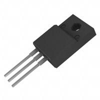
TO-220F
G
MOSFET Maximum Ratings TC = 25oC unless otherwise noted
Symbol
VDSS
Drain to Source Voltage
VGSS
Gate to Source Voltage
S
Parameter
FDPF18N20FT-G
200
Unit
V
±30
V
-Continuous (TC = 25oC)
18*
-Continuous (TC = 100oC)
10.8*
ID
Drain Current
IDM
Drain Current
(Note 1)
72*
A
EAS
Single Pulsed Avalanche Energy
(Note 2)
324
mJ
IAR
Avalanche Current
(Note 1)
18
A
EAR
Repetitive Avalanche Energy
(Note 1)
10
mJ
dv/dt
Peak Diode Recovery dv/dt
(Note 3)
4.5
V/ns
- Pulsed
(TC = 25oC)
PD
Power Dissipation
TJ, TSTG
Operating and Storage Temperature Range
Maximum Lead Temperature for Soldering Purpose,
1/8” from Case for 5 Seconds
TL
- Derate above 25oC
A
35
W
0.27
W/oC
-55 to +150
oC
300
o
FDPF18N20FT-G
Unit
C
*Drain current limited by maximum junction temperature
Thermal Characteristics
Symbol
Parameter
RθJC
Thermal Resistance, Junction to Case, Max.
3.6
RθCS
Thermal Resistance, Case to Sink, Typ.
0.5
RθJA
Thermal Resistance, Junction to Ambient, Max.
62.5
©2012 Semiconductor Components Industries, LLC.
September-2017, Rev. 3
1
oC/W
Publication Order Number:
FDPF18N20FT-G/D
FDPF18N20FT-G N-Channel UniFETTM FRFET® MOSFET
FDPF18N20FT-G
�Device Marking
FDPF18N20FT
Device
FDPF18N20F-G
Package
TO-220F
Eco Status
Green/RoHS
Reel Size
-
Tape Width
-
Quantity
50
Electrical Characteristics
Symbol
Parameter
Test Conditions
Min.
Typ.
Max.
Unit
Off Characteristics
BVDSS
∆BVDSS
∆TJ
Drain to Source Breakdown Voltage
Breakdown Voltage Temperature
Coefficient
ID = 250µA, VGS = 0V, TJ = 25oC
200
-
-
V
ID = 250µA, Referenced to 25oC
-
0.2
-
V/oC
IDSS
Zero Gate Voltage Drain Current
VDS = 200V, VGS = 0V
-
-
10
VDS = 160V, TC = 125oC
-
-
100
IGSS
Gate to Body Leakage Current
VGS = ±30V, VDS = 0V
-
-
±100
3.0
-
5.0
V
-
0.12
0.14
Ω
-
13.6
-
S
-
885
1180
pF
-
200
270
pF
-
24
35
pF
-
20
26
nC
-
5
-
nC
-
9
-
nC
-
16
40
ns
-
50
110
ns
-
50
110
ns
-
40
90
ns
µA
nA
On Characteristics
VGS(th)
RDS(on)
Gate Threshold Voltage
VGS = VDS, ID = 250µA
Static Drain to Source On Resistance
VGS = 10V, ID = 9A
gFS
Forward Transconductance
VDS = 20V, ID = 9A
(Note 4)
Dynamic Characteristics
Ciss
Input Capacitance
Coss
Output Capacitance
Crss
Reverse Transfer Capacitance
Qg(tot)
Total Gate Charge at 10V
Qgs
Gate to Source Gate Charge
Qgd
Gate to Drain “Miller” Charge
VDS = 25V, VGS = 0V
f = 1MHz
VDS = 160V, ID = 18A
VGS = 10V
(Note 4, 5)
Switching Characteristics
td(on)
Turn-On Delay Time
tr
Turn-On Rise Time
td(off)
Turn-Off Delay Time
tf
Turn-Off Fall Time
VDD = 100V, ID = 18A
RG = 25Ω
(Note 4, 5)
Drain-Source Diode Characteristics
IS
Maximum Continuous Drain to Source Diode Forward Current
-
-
18
A
ISM
Maximum Pulsed Drain to Source Diode Forward Current
-
-
72
A
VSD
Drain to Source Diode Forward Voltage
VGS = 0V, ISD = 18A
-
-
1.5
V
trr
Reverse Recovery Time
-
80
-
ns
Qrr
Reverse Recovery Charge
VGS = 0V, ISD = 18A
dIF/dt = 100A/µs
-
240
-
nC
Notes:
1. Repetitive Rating: Pulse width limited by maximum junction temperature
2. L = 2mH, IAS = 18A, VDD = 50V, RG = 25Ω, Starting TJ = 25°C
3. ISD ≤ 18A, di/dt ≤ 200A/µs, VDD ≤ BVDSS, Starting TJ = 25°C
4. Pulse Test: Pulse width ≤ 300µs, Duty Cycle ≤ 2%
5. Essentially Independent of Operating Temperature Typical Characteristics
www.onsemi.com
2
(Note 4)
FDPF18N20FT-G N-Channel UniFETTM FRFET® MOSFET
Package Marking and Ordering Information TC = 25oC unless otherwise noted
�Figure 1. On-Region Characteristics
Figure 2. Transfer Characteristics
30
VGS = 10.0V
8.0 V
7.0 V
6.5 V
6.0 V
5.5 V
10
ID,Drain Current[A]
ID,Drain Current[A]
50
o
10
150 C
o
25 C
*Notes:
1. 250µs Pulse Test
1
*Notes:
1. VDS = 20V
2. 250µs Pulse Test
o
2. TC = 25 C
1
0.1
1
VDS,Drain-Source Voltage[V]
10
4
5
6
VGS,Gate-Source Voltage[V]
0.25
100
IS, Reverse Drain Current [A]
Figure 4. Body Diode Forward Voltage
Variation vs. Source Current
and Temperature
RDS(ON) [Ω],
Drain-Source On-Resistance
Figure 3. On-Resistance Variation vs.
Drain Current and Gate Voltage
0.20
VGS = 10V
VGS = 20V
0.15
o
150 C
o
25 C
10
*Notes:
1. VGS = 0V
o
*Note: TJ = 25 C
2. 250µs Pulse Test
0.10
0
10
20
30
ID, Drain Current [A]
40
1
0.0
50
Figure 5. Capacitance Characteristics
VGS, Gate-Source Voltage [V]
1000
*Note:
1. VGS = 0V
2. f = 1MHz
Ciss
Coss
500
VDS = 40V
VDS = 100V
VDS = 160V
8
6
4
2
Crss
0
0.1
2.0
10
Ciss = Cgs + Cgd (Cds = shorted)
Coss = Cds + Cgd
Crss = Cgd
1500
0.4
0.8
1.2
1.6
VSD, Body Diode Forward Voltage [V]
Figure 6. Gate Charge Characteristics
2000
Capacitances [pF]
7
*Note: ID = 18A
0
1
10
VDS, Drain-Source Voltage [V]
30
0
www.onsemi.com
3
6
12
18
Qg, Total Gate Charge [nC]
24
FDPF18N20FT-G N-Channel UniFETTM FRFET® MOSFET
Typical Performance Characteristics
�Figure 7. Breakdown Voltage Variation
vs. Temperature
Figure 8. Maximum Safe Operating Area
- FDP18N20F
100
20µs
ID, Drain Current [A]
BVDSS, [Normalized]
Drain-Source Breakdown Voltage
1.2
1.1
1.0
100µs
10
1ms
Operation in This Area
is Limited by R DS(on)
1
DC
*Notes:
0.1
0.9
o
1. TC = 25 C
*Notes:
1. VGS = 0V
2. ID = 250µA
0.8
-100
10ms
o
2. TJ = 150 C
3. Single Pulse
0.01
-50
0
50
100
150
o
TJ, Junction Temperature [ C]
1
200
10
100
VDS, Drain-Source Voltage [V]
Figure 9. Maximum Drain Current
vs. Case Temperature
20
12
8
4
0
25
50
75
100
125
o
TC, Case Temperature [ C]
150
Figure 10. Transient Thermal Response Curve - FDP18N20F
2
1
Thermal Response [ZθJC]
ID, Drain Current [A]
16
0.5
0.2
0.1
PDM
0.1
t1
0.05
t2
0.02
*Notes:
0.01
0.01
o
1. ZθJC(t) = 3.0 C/W Max.
2. Duty Factor, D= t1/t2
3. TJM - TC = PDM * ZθJC(t)
Single pulse
-5
10
-4
10
-3
-2
-1
10
10
10
1
Rectangular Pulse Duration [sec]
www.onsemi.com
4
10
2
10
600
FDPF18N20FT-G N-Channel UniFETTM FRFET® MOSFET
Typical Performance Characteristics (Continued)
�Resistive Switching Test Circuit & Waveforms
Unclamped Inductive Switching Test Circuit & Waveforms
www.onsemi.com
5
FDPF18N20FT-G N-Channel UniFETTM FRFET® MOSFET
Gate Charge Test Circuit & Waveform
�DUT
+
VDS
_
I SD
L
Driver
RG
VGS
VGS
( Driver )
Same Type
as DUT
VDD
• dv/dt controlled by RG
• ISD controlled by pulse period
Gate Pulse Width
D = -------------------------Gate Pulse Period
10V
IFM , Body Diode Forward Current
I SD
( DUT )
di/dt
IRM
Body Diode Reverse Current
VDS
( DUT )
Body Diode Recovery dv/dt
VSD
Body Diode
Forward Voltage Drop
www.onsemi.com
6
VDD
FDPF18N20FT-G N-Channel UniFETTM FRFET® MOSFET
Peak Diode Recovery dv/dt Test Circuit & Waveforms
�FDPF18N20FT-G N-Channel UniFETTM FRFET® MOSFET
Mechanical Dimensions
TO-220M03
Dimensions in Millimeters
www.onsemi.com
7
�ON Semiconductor and
are trademarks of Semiconductor Components Industries, LLC dba ON Semiconductor or its subsidiaries in the United States and/or other countries.
ON Semiconductor owns the rights to a number of patents, trademarks, copyrights, trade secrets, and other intellectual property. A listing of ON Semiconductor’s product/patent
coverage may be accessed at www.onsemi.com/site/pdf/Patent−Marking.pdf. ON Semiconductor reserves the right to make changes without further notice to any products herein.
ON Semiconductor makes no warranty, representation or guarantee regarding the suitability of its products for any particular purpose, nor does ON Semiconductor assume any liability
arising out of the application or use of any product or circuit, and specifically disclaims any and all liability, including without limitation special, consequential or incidental damages.
Buyer is responsible for its products and applications using ON Semiconductor products, including compliance with all laws, regulations and safety requirements or standards,
regardless of any support or applications information provided by ON Semiconductor. “Typical” parameters which may be provided in ON Semiconductor data sheets and/or
specifications can and do vary in different applications and actual performance may vary over time. All operating parameters, including “Typicals” must be validated for each customer
application by customer’s technical experts. ON Semiconductor does not convey any license under its patent rights nor the rights of others. ON Semiconductor products are not
designed, intended, or authorized for use as a critical component in life support systems or any FDA Class 3 medical devices or medical devices with a same or similar classification
in a foreign jurisdiction or any devices intended for implantation in the human body. Should Buyer purchase or use ON Semiconductor products for any such unintended or unauthorized
application, Buyer shall indemnify and hold ON Semiconductor and its officers, employees, subsidiaries, affiliates, and distributors harmless against all claims, costs, damages, and
expenses, and reasonable attorney fees arising out of, directly or indirectly, any claim of personal injury or death associated with such unintended or unauthorized use, even if such
claim alleges that ON Semiconductor was negligent regarding the design or manufacture of the part. ON Semiconductor is an Equal Opportunity/Affirmative Action Employer. This
literature is subject to all applicable copyright laws and is not for resale in any manner.
PUBLICATION ORDERING INFORMATION
LITERATURE FULFILLMENT:
Literature Distribution Center for ON Semiconductor
19521 E. 32nd Pkwy, Aurora, Colorado 80011 USA
Phone: 303−675−2175 or 800−344−3860 Toll Free USA/Canada
Fax: 303−675−2176 or 800−344−3867 Toll Free USA/Canada
Email: orderlit@onsemi.com
❖
© Semiconductor Components Industries, LLC
N. American Technical Support: 800−282−9855 Toll Free
USA/Canada
Europe, Middle East and Africa Technical Support:
Phone: 421 33 790 2910
Japan Customer Focus Center
Phone: 81−3−5817−1050
ON Semiconductor Website: www.onsemi.com
Order Literature: http://www.onsemi.com/orderlit
For additional information, please contact your local
Sales Representative
www.onsemi.com
�