ON Semiconductor
Is Now
To learn more about onsemi™, please visit our website at
www.onsemi.com
onsemi and and other names, marks, and brands are registered and/or common law trademarks of Semiconductor Components Industries, LLC dba “onsemi” or its affiliates and/or
subsidiaries in the United States and/or other countries. onsemi owns the rights to a number of patents, trademarks, copyrights, trade secrets, and other intellectual property. A listing of onsemi
product/patent coverage may be accessed at www.onsemi.com/site/pdf/Patent-Marking.pdf. onsemi reserves the right to make changes at any time to any products or information herein, without
notice. The information herein is provided “as-is” and onsemi makes no warranty, representation or guarantee regarding the accuracy of the information, product features, availability, functionality,
or suitability of its products for any particular purpose, nor does onsemi assume any liability arising out of the application or use of any product or circuit, and specifically disclaims any and all
liability, including without limitation special, consequential or incidental damages. Buyer is responsible for its products and applications using onsemi products, including compliance with all laws,
regulations and safety requirements or standards, regardless of any support or applications information provided by onsemi. “Typical” parameters which may be provided in onsemi data sheets and/
or specifications can and do vary in different applications and actual performance may vary over time. All operating parameters, including “Typicals” must be validated for each customer application
by customer’s technical experts. onsemi does not convey any license under any of its intellectual property rights nor the rights of others. onsemi products are not designed, intended, or authorized
for use as a critical component in life support systems or any FDA Class 3 medical devices or medical devices with a same or similar classification in a foreign jurisdiction or any devices intended for
implantation in the human body. Should Buyer purchase or use onsemi products for any such unintended or unauthorized application, Buyer shall indemnify and hold onsemi and its officers, employees,
subsidiaries, affiliates, and distributors harmless against all claims, costs, damages, and expenses, and reasonable attorney fees arising out of, directly or indirectly, any claim of personal injury or death
associated with such unintended or unauthorized use, even if such claim alleges that onsemi was negligent regarding the design or manufacture of the part. onsemi is an Equal Opportunity/Affirmative
Action Employer. This literature is subject to all applicable copyright laws and is not for resale in any manner. Other names and brands may be claimed as the property of others.
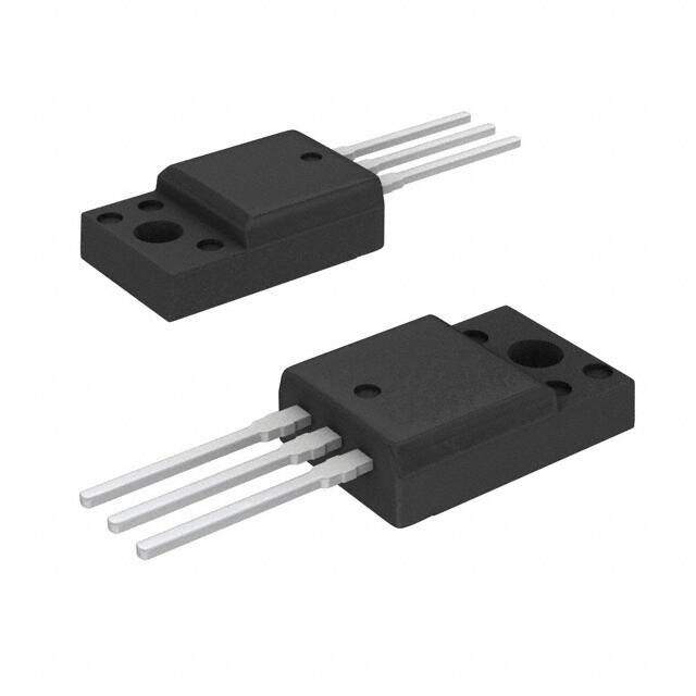
�FDP8D5N10C / FDPF8D5N10C
N-Channel Shielded Gate PowerTrench® MOSFET
100 V, 76 A, 8.5 mΩ
Features
General Description
This N-Channel MV MOSFET is produced using ON
Semiconductor’s advanced PowerTrench® process that
incorporates Shielded Gate technology. This process has been
optimized to minimize on-state resistance and yet maintain
superior switching performance with best in class soft body
diode.
Max rDS(on) = 8.5 mΩ at VGS = 10 V, ID = 76 A
Extremely Low Reverse Recovery Charge, Qrr
100% UIL Tested
RoHS Compliant
Applications
Synchronous Rectification for ATX / Server / Telecom PSU
Motor drives and Uninterruptible Power Supplies
Micro Solar Inverter
D
G
G
G
D
S
D
S
TO-220
S
TO-220F
MOSFET Maximum Ratings TC = 25 °C unless otherwise noted.
Symbol
Ratings
Parameter
VDS
Drain to Source Voltage
FDP8D5N10C
100
VGS
Gate to Source Voltage
±20
±20
76
76*
Drain Current -Continuous
ID
-Continuous
TC = 25°C
(Note 3)
TC = 100°C
(Note 3)
54
54*
(Note 1)
304
304*
-Pulsed
Single Pulse Avalanche Energy
EAS
PD
TJ, TSTG
FDPF8D5N10C
100
(Note 2)
Units
V
V
A
181
mJ
Power Dissipation
TC = 25°C
107
35
Power Dissipation
TA = 25°C
2.4
2.4
-55 to +175
-55 to +175
°C
Units
Operating and Storage Junction Temperature Range
W
* Drain current limited by maximum junction temperature.
Thermal Characteristics
FDP8D5N10C
FDPF8D5N10C
RθJC
Symbol
Thermal Resistance, Junction to Case
Parameter
1.4
4.2
RθJA
Thermal Resistance, Junction to Ambient
62.5
62.5
°C/W
Package Marking and Ordering Information
Device Marking
FDP8D5N10C
Device
FDP8D5N10C
Package
TO-220
Reel Size
-
Tape Width
-
Quantity
50 units
FDPF8D5N10C
FDPF8D5N10C
TO-220F
-
-
50 units
Semiconductor Components Industries, LLC, 2017
May, 2017, Rev. 1.0
Publication Order Number:
FDP8D5N10C / FDPF8D5N10C/D
1
FDP8D5N10C / FDPF8D5N10C N-Channel Shielded Gate PowerTrench® MOSFET
www.onsemi.com
�Symbol
Parameter
Test Conditions
Min.
Typ.
Max.
Units
Off Characteristics
BVDSS
Drain to Source Breakdown Voltage
ID = 250 μA, VGS = 0 V
ΔBVDSS
ΔTJ
Breakdown Voltage Temperature
Coefficient
ID = 250 μA, referenced to 25 °C
IDSS
Zero Gate Voltage Drain Current
IGSS
Gate to Source Leakage Current
100
V
57
mV/°C
VDS = 80 V, VGS = 0 V
1
μA
VDS = 80 V, TJ= 150°C
500
μA
VGS = ±20 V, VDS = 0 V
±100
nA
On Characteristics
VGS(th)
Gate to Source Threshold Voltage
VGS = VDS, ID = 130 μA
3.0
4.0
V
rDS(on)
Static Drain to Source On Resistance
VGS = 10 V, ID = 76 A
7.4
8.5
mΩ
gFS
Forward Transconductance
VDS = 5 V, ID = 76 A
68
2.0
S
Dynamic Characteristics
Ciss
Input Capacitance
Coss
Output Capacitance
Crss
Reverse Transfer Capacitance
Rg
Gate Resistance
VDS = 50 V, VGS = 0 V,
f = 1 MHz
0.1
1765
2475
pF
1010
1415
pF
16
25
pF
0.8
1.6
Ω
12
22
ns
11
20
ns
18
28
ns
4
10
ns
25
34
Switching Characteristics
td(on)
Turn-On Delay Time
tr
Rise Time
td(off)
Turn-Off Delay Time
tf
Fall Time
Qg
Total Gate Charge
Qgs
Gate to Source Gate Charge
Qgd
Gate to Drain “Miller” Charge
Qoss
Output Charge
VDD = 50 V, ID = 76 A,
VGS = 10 V, RGEN = 6 Ω
VGS = 0 V to 10 V
VDD = 50 V,
ID = 76 A
VDD = 50 V, VGS = 0 V
nC
9
nC
5
nC
68
nC
Drain-Source Diode Characteristic
IS
Maximum Continuous Drain to Source Diode Forward Current
-
-
76
A
ISM
Maximum Pulsed Drain to Source Diode Forward Current
-
-
304
A
VSD
Source to Drain Diode Forward Voltage
VGS = 0 V, IS = 76 A
1.0
1.3
V
trr
Reverse Recovery Time
VGS = 0 V, VDD = 50 V, IF = 76 A,
dIF/dt = 100 A/μs
58
92
ns
53
85
nC
51
81
ns
141
226
nC
Qrr
Reverse Recovery Charge
trr
Reverse Recovery Time
Qrr
Reverse Recovery Charge
VGS = 0 V, VDD = 50 V, IF = 76 A,
dIF/dt = 300 A/μs
Notes:
1. Pulsed Id please refer to Figure 11 & Figure 12 “Forward Bias Safe Operating Area” for more details.
2. EAS of 181 mJ is based on starting TJ = 25 °C, L = 3 mH, IAS = 11 A, VDD = 100 V, VGS = 10 V. 100% test at L = 0.3 mH, IAS = 25 A.
3. Computed continuous current limited to Max Junction Temperature only, actual continuous current will be limited by thermal & electro-mechanical application board design.
www.onsemi.com
2
FDP8D5N10C / FDPF8D5N10C N-Channel Shielded Gate PowerTrench® MOSFET
Electrical Characteristics TJ = 25 °C unless otherwise noted.
�VGS = 10 V PULSE DURATION = 80 μs
DUTY CYCLE = 0.5% MAX
VGS = 8 V
120
VGS = 6 V
90
VGS = 5.5 V
60
30
0
VGS = 5 V
0
1
2
3
4
6.0
NORMALIZED
DRAIN TO SOURCE ON-RESISTANCE
ID, DRAIN CURRENT (A)
150
VGS = 5 V
4.5
VGS = 5.5 V
VGS = 6 V
3.0
VGS = 8 V
1.5
0.0
5
0
30
VDS, DRAIN TO SOURCE VOLTAGE (V)
80
ID = 76 A
VGS = 10 V
2.0
rDS(on), DRAIN TO
1.8
1.6
1.4
1.2
1.0
0.8
SOURCE ON-RESISTANCE (mΩ)
NORMALIZED
DRAIN TO SOURCE ON-RESISTANCE
90
0.6
-75 -50 -25 0
25 50 75 100 125 150 175
TJ, JUNCTION TEMPERATURE (oC)
IS, REVERSE DRAIN CURRENT (A)
VDS = 5 V
90
TJ = 175 oC
TJ = 25 oC
TJ = -55 oC
2
4
6
50
40
30
TJ = 150 oC
20
10
TJ = 25 oC
5
6
7
8
9
10
Figure 4. On-Resistance vs. Gate to
Source Voltage
PULSE DURATION = 80 μs
DUTY CYCLE = 0.5% MAX
30
ID = 76 A
60
VGS, GATE TO SOURCE VOLTAGE (V)
150
60
150
PULSE DURATION = 80 μs
DUTY CYCLE = 0.5% MAX
70
0
Figure 3. Normalized On Resistance
vs. Junction Temperature
120
120
Figure 2. Normalized On-Resistance
vs. Drain Current and Gate Voltage
2.2
ID, DRAIN CURRENT (A)
60
ID, DRAIN CURRENT (A)
Figure 1. On Region Characteristics
0
PULSE DURATION = 80 μs
DUTY CYCLE = 0.5% MAX
VGS = 10 V
200
100
VGS = 0 V
10
TJ = 175 oC
1
TJ = 25 oC
0.1
TJ = -55 oC
0.01
0.001
0.0
8
0.2
0.4
0.6
0.8
1.0
VGS, GATE TO SOURCE VOLTAGE (V)
VSD, BODY DIODE FORWARD VOLTAGE (V)
Figure 5. Transfer Characteristics
Figure 6. Source to Drain Diode
Forward Voltage vs. Source Current
www.onsemi.com
3
1.2
FDP8D5N10C / FDPF8D5N10C N-Channel Shielded Gate PowerTrench® MOSFET
Typical Characteristics TJ = 25 °C unless otherwise noted.
�10000
ID = 76 A
Ciss
VDD = 25 V
8
VDD = 50 V
CAPACITANCE (pF)
VGS, GATE TO SOURCE VOLTAGE (V)
10
VDD = 75 V
6
4
1000
100
Crss
10
2
0
Coss
f = 1 MHz
VGS = 0 V
0
6
12
18
24
1
0.1
30
1
Figure 7. Gate Charge Characteristics
90
ID, DRAIN CURRENT (A)
IAS, AVALANCHE CURRENT (A)
100
Figure 8. Capacitance vs. Drain
to Source Voltage
50
TJ = 25 oC
10
TJ =
TJ = 150
1
0.01
0.1
125 oC
oC
1
75
60
VGS = 10 V
45
30
o
RθJC = 1.4 C/W
15
10
0
25
100
50
75
100
125
150
175
o
tAV, TIME IN AVALANCHE (ms)
TC, CASE TEMPERATURE ( C)
Figure 9. Unclamped Inductive
Switching Capability
Figure 10. Maximum Continuous Drain Current vs.
Case Temperature for FDP8D5N10C
500
100
ID, DRAIN CURRENT (A)
500
ID, DRAIN CURRENT (A)
10
VDS, DRAIN TO SOURCE VOLTAGE (V)
Qg, GATE CHARGE (nC)
10 μs
10
THIS AREA IS
LIMITED BY rDS(on)
100 μs
SINGLE PULSE
TJ = MAX RATED
1
RθJC = 1.4 oC/W
0.1
0.1
TC = 25 oC
1
1 ms
10 μs
10
THIS AREA IS
LIMITED BY rDS(on)
100
RθJC = 4.2 oC/W
0.1
0.1
400
100 μs
SINGLE PULSE
TJ = MAX RATED
1
10 ms
100 ms
CURVE BENT TO
MEASURED DATA
10
100
TC = 25 oC
1
1 ms
10 ms
100 ms
CURVE BENT TO
MEASURED DATA
10
100
VDS, DRAIN to SOURCE VOLTAGE (V)
VDS, DRAIN to SOURCE VOLTAGE (V)
Figure 12. Forward Bias Safe
Operating Area for FDPF8D5N10C
Figure 11. Forward Bias Safe
Operating Area for FDP8D5N10C
www.onsemi.com
4
400
FDP8D5N10C / FDPF8D5N10C N-Channel Shielded Gate PowerTrench® MOSFET
Typical Characteristics TJ = 25 °C unless otherwise noted.
�50000
P(PK), PEAK TRANSIENT POWER (W)
P(PK), PEAK TRANSIENT POWER (W)
50000
SINGLE PULSE
RθJC = 1.4 oC/W
10000
TC = 25 oC
1000
100
10
-5
10
-4
10
-3
10
-2
10
-1
10
0
10
1
10
SINGLE PULSE
RθJC = 4.2 oC/W
10000
TC = 25 oC
1000
2
10
100
10
-5
10
-4
10
-1
0
10
1
10
10
2
10
Figure 14. Single Pulse Maximum Power Dissipation
for FDPF8D5N10C
Figure 13. Single Pulse Maximum Power Dissipation
for FDP8D5N10C
r(t), NORMALIZED EFFECTIVE TRANSIENT
THERMAL RESISTANCE
-2
10
t, PULSE WIDTH (sec)
t, PULSE WIDTH (sec)
2
-3
10
DUTY CYCLE-DESCENDING ORDER
1
D = 0.5
0.2
0.1
0.05
0.02
0.01
0.1
PDM
t1
t2
NOTES:
SINGLE PULSE
0.01
ZθJC(t) = r(t) x RθJC
RθJC = 1.4 oC/W
Peak TJ = PDM x ZθJC(t) + TC
Duty Cycle, D = t1 / t2
0.001
-5
10
-4
10
-3
10
-2
-1
10
10
0
1
10
2
10
10
t, RECTANGULAR PULSE DURATION (sec)
r(t), NORMALIZED EFFECTIVE TRANSIENT
THERMAL RESISTANCE
Figure 15. Junction-to-Case Transient Thermal Response Curve for FDP2D3N10C
2
DUTY CYCLE-DESCENDING ORDER
1
D = 0.5
0.2
0.1
0.05
0.02
0.01
0.1
PDM
t1
t2
0.01
NOTES:
ZθJC(t) = r(t) x RθJC
RθJC = 4.2 oC/W
Peak TJ = PDM x ZθJC(t) + TC
Duty Cycle, D = t1 / t2
SINGLE PULSE
0.001
-5
10
-4
10
-3
10
-2
-1
10
10
0
10
1
10
t, RECTANGULAR PULSE DURATION (sec)
Figure 16. Junction-to-Case Transient Thermal Response Curve for FDPF2D3N10C
www.onsemi.com
5
2
10
FDP8D5N10C / FDPF8D5N10C N-Channel Shielded Gate PowerTrench® MOSFET
Typical Characteristics TJ = 25 °C unless otherwise noted.
�TO-220, Molded, 3-Lead, Jedec Variation AB (Delta)
ON Semiconductor and the ON Logo are trademarks of Semiconductor Components Industries, LLC dba ON Semiconductor or its subsidiaries in the United States and/or other
countries.
ON Semiconductor owns the rights to a number of patents, trademarks, copyrights, trade secrets, and other intellectual property. A listing of ON Semiconductor's product/patent
coverage may be accessed at www.onsemi.com/site/pdf/Patent-Marking.pdf. ON Semiconductor reserves the right to make changes without further notice to any products herein.
ON Semiconductor makes no warranty, representation or guarantee regarding the suitability of its products for any particular purpose, nor does ON Semiconductor assume any
liability arising out of the application or use of any product or circuit, and specifically disclaims any and all liability, including without limitation special, consequential or incidental
damages. Buyer is responsible for its products and applications using ON Semiconductor products, including compliance with all laws, regulations and safety requirements or
standards, regardless of any support or applications information provided by
ON Semiconductor. “Typical” parameters which may be provided in ON Semiconductor data sheets and/or specifications can and do vary in different applications and actual
performance may vary over time. All operating parameters, including “Typicals” must be validated for each customer application by customer's technical experts. ON
Semiconductor does not convey any license under its patent rights nor the rights of others. ON Semiconductor products are not designed, intended, or authorized for use as a
critical component in life support systems or any FDA Class 3 medical devices or medical devices with a same or similar classification in a foreign jurisdiction or any devices
intended for implantation in the human body. Should Buyer purchase or use ON Semiconductor products for any such unintended or unauthorized application, Buyer shall
indemnify and hold ON Semiconductor and its officers, employees, subsidiaries, affiliates, and distributors harmless against all claims, costs, damages, and expenses, and
reasonable attorney fees arising out of, directly or indirectly, any claim of personal injury or death associated with such unintended or unauthorized use, even if such claim alleges
that ON Semiconductor was negligent regarding the design or manufacture of the part. ON Semiconductor is an Equal Opportunity/Affirmative Action Employer. This literature is
subject to all applicable copyright laws and is not for resale in any manner.
www.onsemi.com
6
FDP8D5N10C / FDPF8D5N10C N-Channel Shielded Gate PowerTrench® MOSFET
Dimensional Outline and Pad Layout
�FDP8D5N10C / FDPF8D5N10C N-Channel Shielded Gate PowerTrench® MOSFET
Dimensional Outline and Pad Layout
TO220, Molded, 3-Lead, Full Pack, EIAJ SC91, Straight Lead
ON Semiconductor and the ON Logo are trademarks of Semiconductor Components Industries, LLC dba ON Semiconductor or its subsidiaries in the United States and/or other
countries.
ON Semiconductor owns the rights to a number of patents, trademarks, copyrights, trade secrets, and other intellectual property. A listing of ON Semiconductor's product/patent
coverage may be accessed at www.onsemi.com/site/pdf/Patent-Marking.pdf. ON Semiconductor reserves the right to make changes without further notice to any products herein.
ON Semiconductor makes no warranty, representation or guarantee regarding the suitability of its products for any particular purpose, nor does ON Semiconductor assume any
liability arising out of the application or use of any product or circuit, and specifically disclaims any and all liability, including without limitation special, consequential or incidental
damages. Buyer is responsible for its products and applications using ON Semiconductor products, including compliance with all laws, regulations and safety requirements or
standards, regardless of any support or applications information provided by
ON Semiconductor. “Typical” parameters which may be provided in ON Semiconductor data sheets and/or specifications can and do vary in different applications and actual
performance may vary over time. All operating parameters, including “Typicals” must be validated for each customer application by customer's technical experts. ON
Semiconductor does not convey any license under its patent rights nor the rights of others. ON Semiconductor products are not designed, intended, or authorized for use as a
critical component in life support systems or any FDA Class 3 medical devices or medical devices with a same or similar classification in a foreign jurisdiction or any devices
intended for implantation in the human body. Should Buyer purchase or use ON Semiconductor products for any such unintended or unauthorized application, Buyer shall
indemnify and hold ON Semiconductor and its officers, employees, subsidiaries, affiliates, and distributors harmless against all claims, costs, damages, and expenses, and
reasonable attorney fees arising out of, directly or indirectly, any claim of personal injury or death associated with such unintended or unauthorized use, even if such claim alleges
that ON Semiconductor was negligent regarding the design or manufacture of the part. ON Semiconductor is an Equal Opportunity/Affirmative Action Employer. This literature is
subject to all applicable copyright laws and is not for resale in any manner.
www.onsemi.com
7
�