FDU6676AS
tm
N-Channel PowerTrench® SyncFET™
30V, 90A, 5.8mΩ
General Description
Features
The FDU6676AS is designed to replace a single
MOSFET and Schottky diode in synchronous DC/DC
power supplies. This 30V MOSFET is designed to
maximize power conversion efficiency, providing a low
RDS(ON) and low gate charge. The FDU6676AS includes
a patented combination of a MOSFET monolithically
integrated with a Schottky diode using Fairchild’s
monolithic SyncFET technology.
• RDS(ON) = 5.8mΩ Max, VGS = 10V
• RDS(ON) = 7.3mΩ Max, VGS = 4.5V
• High performance trench technology for extremely
low RDS(ON)
• Low Gate Charge
Applications
• High power and current handling capability
• DC/DC converter
• Includes SyncFET Schottky diode
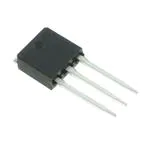
D
G
I-PAK
(TO-251AA)
S
G D S
Absolute Maximum Ratings
Symbol
TA=25oC unless otherwise noted
Ratings
Units
VDSS
Drain-Source Voltage
30
V
VGSS
ID
Gate-Source Voltage
Drain Current
±20
V
A
PD
–Pulsed
Power Dissipation for Single Operation
TJ, TSTG
Parameter
–Continuous
(Note 1a)
90
100
(Note 1)
70
(Note 1a)
3.1
(Note 1b)
1.3
Operating and Storage Junction Temperature
Range
W
–55 to +150
°C
°C/W
Thermal Characteristics
Thermal Resistance junction to Case
RθJC
RθJA
(Note 1)
1.8
Thermal Resistance junction to Ambient
(Note 1a)
45
RθJA
Thermal Resistance junction to Ambient
(Note 1b)
96
Package Marking and Ordering Information
Device Marking
FDU6676AS
FDU6676AS
Device
FDU6676AS
FDU6676AS_F071 (Note 4)
©2008 Fairchild Semiconductor Corporation
Package
I-PAK (TO-251)
I-PAK (TO-251)����
Reel Size
Tube
Tube
Tape width
N/A
N/A
Quantity
75
75
FDU6676AS Rev. A1 (W)
FDU6676AS
April 2008
�Symbol
TA = 25°C unless otherwise noted
Parameter
Test Conditions
Min Typ Max
Units
Single Pulse, VDD = 15V,ID = 16A
108
250
mJ
16
A
Drain-Source Avalanche Ratings (Note 2)
WDSS
Drain-Source Avalanche Energy
IAR
Drain-Source Avalanche Current
Off Characteristics
BVDSS
∆BVDSS
∆TJ
IDSS
IGSS
Drain–Source Breakdown
Voltage
Breakdown Voltage Temperature
Coefficient
Zero Gate Voltage Drain Current
Gate–Body Leakage
On Characteristics
VGS = 0 V,
ID = 250 µA
30
V
ID = 250 µA,Referenced to 25°C
29
VDS = 24 V, VGS = 0 V
VDS = 24 V, VGS = 0 V, TJ=125°C
VGS = ±20 V, VDS = 0 V
13
mV/°C
500
±100
µA
mA
nA
(Note 2)
VGS(th)
∆VGS(th)
∆TJ
RDS(on)
Gate Threshold Voltage
Gate Threshold Voltage
Temperature Coefficient
ID = 250 µA
VDS = VGS,
ID = 250 µA,Referenced to 25°C
Static Drain–Source
On–Resistance
gFS
Forward Transconductance
VGS = 10 V,
ID = 16 A
VGS = 4.5 V, ID = 10 A
VGS = 10 V, ID = 16 A,TJ=125°C
VDS = 10 V,
ID = 16 A
1
1.5
–4
3
V
mV/°C
4.8
5.8
7.7
5.8
7.3
9.6
mΩ
67
S
Dynamic Characteristics
Ciss
Input Capacitance
Coss
Output Capacitance
Crss
RG
Reverse Transfer Capacitance
Gate Resistance
Switching Characteristics
td(on)
Turn–On Delay Time
tr
Turn–On Rise Time
VDS = 15 V,
f = 1.0 MHz
V GS = 0 V,
2470
pF
710
pF
260
pF
VGS = 100 mV, f = 1.0 MHz
1.8
Ω
12
22
ns
VDD = 15 V,
VGS = 10 V,
12
22
ns
(Note 2)
ID = 1 A,
RGEN = 6 Ω
td(off)
Turn–Off Delay Time
50
80
ns
tf
Turn–Off Fall Time
25
40
ns
td(on)
Turn–On Delay Time
20
32
ns
tr
Turn–On Rise Time
24
38
ns
td(off)
Turn–Off Delay Time
34
54
ns
tf
Turn–Off Fall Time
26
42
ns
VDD = 15 V,
VGS = 4.5 V,
ID = 1 A,
RGEN = 6 Ω
Qg
Total Gate Charge, VGS = 10V
46
64
nC
Qg
Total Gate Charge, VGS = 5V
25
35
nC
Qgs
Gate–Source Charge
6
nC
Qgd
Gate–Drain Charge
7
nC
VDS = 15V,
ID = 16 A
FDU6676AS Rev A1 (W)
FDU6676AS
Electrical Characteristics
�Symbol
TA = 25°C unless otherwise noted
Parameter
Test Conditions
Min Typ Max
Units
Drain–Source Diode Characteristics and Maximum Ratings
IS
0.4
trr
Maximum Continuous Drain–Source Diode Forward Current
Drain–Source Diode Forward
(Note 2)
VGS = 0 V, IS = 2.3 A
Voltage
=
16
A,
dI
/dt
=
100
A/µs
I
F
F
Diode Reverse Recovery Time
28
ns
Qrr
Diode Reverse Recovery Charge
19
nC
VSD
2.3
A
1.2
V
Notes:
1. RθJA is the sum of the junction-to-case and case-to-ambient thermal resistance where the case thermal reference is defined as the solder mounting surface of
the drain pins. RθJC is guaranteed by design while RθCA is determined by the user's board design.
a) RθJA = 45°C/W when mounted on a
1in2 pad of 2 oz copper
b) RθJA = 96°C/W when mounted
on a minimum pad.
Scale 1 : 1 on letter size paper
2. Pulse Test: Pulse Width < 300µs, Duty Cycle < 2.0%
3. Maximum current is calculated as:
PD
R DS(ON)
where PD is maximum power dissipation at TC = 25°C and RDS(on) is at TJ(max) and VGS = 10V. Package current limitation is 21A
4. FDU6676AS_F071 is a lead free product. The FDU6676AS_F071 marking will appear on the reel label.
5
FDU6676AS Rev A1 (W)
FDU6676AS
Electrical Characteristics
�FDU6676AS
Typical Characteristics
100
2
VGS = 10V
3.5V
VGS = 3.0V
RDS(ON), NORMALIZED
DRAIN-SOURCE ON-RESISTANCE
ID, DRAIN CURRENT (A)
6.0V
4.0V
80
4.5V
60
3.0V
40
20
2.5V
0
0.5
1
1.5
2
VDS, DRAIN-SOURCE VOLTAGE (V)
3.5V
1.4
4.0V
4.5V
1.2
6.0V
10V
1
2.5
0
Figure 1. On-Region Characteristics
20
40
60
ID, DRAIN CURRENT (A)
80
100
Figure 2. On-Resistance Variation with
Drain Current and Gate Voltage
0.0175
1.6
ID = 16A
VGS = 10V
ID = 8A
RDS(ON), ON-RESISTANCE (OHM)
RDS(ON), NORMALIZED
DRAIN-SOURCE ON-RESISTANCE
1.6
0.8
0
1.4
1.2
1
0.8
0.015
0.0125
o
0.01
TA = 125 C
0.0075
o
TA = 25 C
0.005
0.0025
0.6
-50
-25
0
25
50
75
100
o
TJ, JUNCTION TEMPERATURE ( C)
125
2
150
Figure 3. On-Resistance Variation with
Temperature
4
6
8
VGS, GATE TO SOURCE VOLTAGE (V)
10
Figure 4. On-Resistance Variation with
Gate-to-Source Voltage
100
100
VGS = 0V
IS, REVERSE DRAIN CURRENT (A)
VDS = 5V
80
ID, DRAIN CURRENT (A)
1.8
60
o
40
TA =125 C
-55oC
20
10
1
o
TA = 125 C
0.1
25oC
0.01
o
-55 C
0.001
25oC
0.0001
0
1
1.5
2
2.5
3
3.5
VGS, GATE TO SOURCE VOLTAGE (V)
Figure 5. Transfer Characteristics
4
0
0.2
0.4
0.6
0.8
VSD, BODY DIODE FORWARD VOLTAGE (V)
1
Figure 6. Body Diode Forward Voltage Variation
with Source Current and Temperature
FDU6676AS Rev A1 (W)
�3500
ID = 16A
f = 1MHz
VGS = 0 V
3000
8
VDS = 10V
2500
CAPACITANCE (pF)
VGS, GATE-SOURCE VOLTAGE (V)
10
20V
6
Ciss
2000
15V
1500
4
Coss
1000
2
500
Crss
0
0
0
10
20
30
Qg, GATE CHARGE (nC)
40
0
50
Figure 7. Gate Charge Characteristics
10
15
20
25
VDS, DRAIN TO SOURCE VOLTAGE (V)
30
Figure 8. Capacitance Characteristics
100
100
P(pk), PEAK TRANSIENT POWER (W)
1000
100µs
RDS(ON) LIMIT
1m
10ms
10
100ms
1s
10s
1
DC
VGS = 10V
SINGLE PULSE
RθJA = 96oC/W
0.1
o
TA = 25 C
0.01
0.01
0.1
1
10
VDS, DRAIN-SOURCE VOLTAGE (V)
60
40
20
0
0.01
100
SINGLE PULSE
RθJA = 96°C/W
TA = 25°C
80
Figure 9. Maximum Safe Operating Area
r(t), NORMALIZED EFFECTIVE
TRANSIENT THERMAL RESISTANCE
ID, DRAIN CURRENT (A)
5
0.1
1
10
t1, TIME (sec)
100
1000
Figure 10. Single Pulse Maximum
Power Dissipation
1
D = 0.5
RθJA(t) = r(t) * RθJA
RθJA = 96 °C/W
0.2
0.1
0.1
0.05
P(pk)
0.02
t1
0.01
t2
0.01
TJ - TA = P * RθJA(t)
Duty Cycle, D = t1 / t2
SINGLE PULSE
0.001
0.001
0.01
0.1
1
10
100
1000
t1, TIME (sec)
Figure 11. Transient Thermal Response Curve
Thermal characterization performed using the conditions described in Note 1b.
Transient thermal response will change depending on the circuit board design.
FDU6676AS Rev A1 (W)
FDU6676AS
Typical Characteristics
�FDU6676AS
Typical Characteristics (continued)
SyncFET Schottky Body Diode
Characteristics
Schottky barrier diodes exhibit significant leakage at
high temperature and high reverse voltage. This will
increase the power in the device.
IDSS, REVERSE LEAKAGE CURRENT (A)
CURRENT : 0.8A/div
Fairchild’s SyncFET process embeds a Schottky diode
in parallel with PowerTrench MOSFET. This diode
exhibits similar characteristics to a discrete external
Schottky diode in parallel with a MOSFET. Figure 12
shows the reverse recovery characteristic of the
FDU6676AS.
0.1
125oC
0.01
100oC
0.001
0.0001
25oC
0.00001
0
10
20
VDS, REVERSE VOLTAGE (V)
30
Figure 14. SyncFET Body Diode Reverse
Leakage Versus Drain-Source Voltage and
Temperature.
TIME : 12.5ns/div
Figure 12. FDU6676AS SyncFET Body Diode
Reverse Recovery Characteristic.
CURRENT : 0.8A/div
For comparison purposes, Figure 13 shows the reverse
recovery characteristics of the body diode of an
equivalent size MOSFET produced without SyncFET
(FDU6676A).
TIME : 12.5ns/div
Figure 13. Non-SyncFET (FDU6676A) Body
Biode Reverse Recovery Characteristic.
FDU6676AS Rev A1 (W)
�The following includes registered and unregistered trademarks and service marks, owned by Fairchild Semiconductor and/or its global
subsidianries, and is not intended to be an exhaustive list of all such trademarks.
ACEx®
Build it Now™
CorePLUS™
CorePOWER™
CROSSVOLT™
CTL™
Current Transfer Logic™
EcoSPARK®
EfficentMax™
EZSWITCH™ *
FPS™
F-PFS™
FRFET®
Global Power ResourceSM
Green FPS™
Green FPS™ e-Series™
GTO™
IntelliMAX™
ISOPLANAR™
MegaBuck™
MICROCOUPLER™
MicroFET™
MicroPak™
MillerDrive™
MotionMax™
Motion-SPM™
OPTOLOGIC®
OPTOPLANAR®
™
®
Fairchild®
Fairchild Semiconductor®
FACT Quiet Series™
FACT®
FAST®
FastvCore™
FlashWriter® *
®
PDP-SPM™
Power-SPM™
PowerTrench®
Programmable Active Droop™
QFET®
QS™
Quiet Series™
RapidConfigure™
Saving our world 1mW at a time™
SmartMax™
SMART START™
SPM®
STEALTH™
SuperFET™
SuperSOT™-3
SuperSOT™-6
SuperSOT™-8
SuperMOS™
®
The Power Franchise®
tm
TinyBoost™
TinyBuck™
TinyLogic®
TINYOPTO™
TinyPower™
TinyPWM™
TinyWire™
µSerDes™
UHC®
Ultra FRFET™
UniFET™
VCX™
VisualMax™
tm
* EZSWITCH™ and FlashWriter® are trademarks of System General Corporation, used under license by Fairchild Semiconductor.
DISCLAIMER
FAIRCHILD SEMICONDUCTOR RESERVES THE RIGHT TO MAKE CHANGES WITHOUT FURTHER NOTICE TO ANY PRODUCTS
HEREIN TO IMPROVE RELIABILITY, FUNCTION, OR DESIGN. FAIRCHILD DOES NOT ASSUME ANY LIABILITY ARISING OUT OF THE
APPLICATION OR USE OF ANY PRODUCT OR CIRCUIT DESCRIBED HEREIN; NEITHER DOES IT CONVEY ANY LICENSE UNDER
ITS PATENT RIGHTS, NOR THE RIGHTS OF OTHERS. THESE SPECIFICATIONS DO NOT EXPAND THE TERMS OF FAIRCHILD’S
WORLDWIDE TERMS AND CONDITIONS, SPECIFICALLY THE WARRANTY THEREIN, WHICH COVERS THESE PRODUCTS.
LIFE SUPPORT POLICY
FAIRCHILD’S PRODUCTS ARE NOT AUTHORIZED FOR USE AS CRITICAL COMPONENTS IN LIFE SUPPORT DEVICES OR
SYSTEMS WITHOUT THE EXPRESS WRITTEN APPROVAL OF FAIRCHILD SEMICONDUCTOR CORPORATION.
As used herein:
1.
Life support devices or systems are devices or systems which,
(a) are intended for surgical implant into the body or (b)
support or sustain life, and (c) whose failure to perform when
properly used in accordance with instructions for use provided
in the labeling, can be reasonably expected to result in a
significant injury of the user.
2.
A critical component in any component of a life support,
device, or system whose failure to perform can be reasonably
expected to cause the failure of the life support device or
system, or to affect its safety or effectiveness.
PRODUCT STATUS DEFINITIONS
Definition of Terms
Datasheet Identification
Product Status
Definition
Advance Information
Formative or In Design
This datasheet contains the design specifications for product development.
Specifications may change in any manner without notice.
Preliminary
First Production
This datasheet contains preliminary data; supplementary data will be published at a later date. Fairchild Semiconductor reserves the right to make
changes at any time without notice to improve design.
No Identification Needed
Full Production
This datasheet contains final specifications. Fairchild Semiconductor reserves
the right to make changes at any time without notice to improve the design.
Obsolete
Not In Production
This datasheet contains specifications on a product that is discontinued by
Fairchild Semiconductor. The datasheet is for reference information only.
Rev. I34
FDU6676AS Rev A1 (W)
FDU6676AS
TRADEMARKS
�


 工商网监
湘ICP备2023018690号
工商网监
湘ICP备2023018690号

