Is Now Part of
To learn more about ON Semiconductor, please visit our website at
www.onsemi.com
Please note: As part of the Fairchild Semiconductor integration, some of the Fairchild orderable part numbers
will need to change in order to meet ON Semiconductor’s system requirements. Since the ON Semiconductor
product management systems do not have the ability to manage part nomenclature that utilizes an underscore
(_), the underscore (_) in the Fairchild part numbers will be changed to a dash (-). This document may contain
device numbers with an underscore (_). Please check the ON Semiconductor website to verify the updated
device numbers. The most current and up-to-date ordering information can be found at www.onsemi.com. Please
email any questions regarding the system integration to Fairchild_questions@onsemi.com.
ON Semiconductor and the ON Semiconductor logo are trademarks of Semiconductor Components Industries, LLC dba ON Semiconductor or its subsidiaries in the United States and/or other countries. ON Semiconductor owns the rights to a number
of patents, trademarks, copyrights, trade secrets, and other intellectual property. A listing of ON Semiconductor’s product/patent coverage may be accessed at www.onsemi.com/site/pdf/Patent-Marking.pdf. ON Semiconductor reserves the right
to make changes without further notice to any products herein. ON Semiconductor makes no warranty, representation or guarantee regarding the suitability of its products for any particular purpose, nor does ON Semiconductor assume any liability
arising out of the application or use of any product or circuit, and specifically disclaims any and all liability, including without limitation special, consequential or incidental damages. Buyer is responsible for its products and applications using ON
Semiconductor products, including compliance with all laws, regulations and safety requirements or standards, regardless of any support or applications information provided by ON Semiconductor. “Typical” parameters which may be provided in ON
Semiconductor data sheets and/or specifications can and do vary in different applications and actual performance may vary over time. All operating parameters, including “Typicals” must be validated for each customer application by customer’s
technical experts. ON Semiconductor does not convey any license under its patent rights nor the rights of others. ON Semiconductor products are not designed, intended, or authorized for use as a critical component in life support systems or any FDA
Class 3 medical devices or medical devices with a same or similar classification in a foreign jurisdiction or any devices intended for implantation in the human body. Should Buyer purchase or use ON Semiconductor products for any such unintended
or unauthorized application, Buyer shall indemnify and hold ON Semiconductor and its officers, employees, subsidiaries, affiliates, and distributors harmless against all claims, costs, damages, and expenses, and reasonable attorney fees arising out
of, directly or indirectly, any claim of personal injury or death associated with such unintended or unauthorized use, even if such claim alleges that ON Semiconductor was negligent regarding the design or manufacture of the part. ON Semiconductor
is an Equal Opportunity/Affirmative Action Employer. This literature is subject to all applicable copyright laws and is not for resale in any manner.
�January 2007
FDY3000NZ
tm
DualN-Channel2.5V Specified PowerTrench MOSFET
GeneralDescription
Features
Thi
s Dual N-Channel MOSFET has been desi
gned
usi
ng Fai
rchi
l
d Semi
conductor’
s advanced Power
Trench process to opti
mi
ze the RDS(ON)@ VGS = 2.5v.
x 600 mA,20 V RDS(ON)= 700 m:�@ VGS = 4.5 V
Applications
x ESD protecti
on di
ode (note 3)
x Li
-Ion Battery Pack
x RoHS Compl
i
ant
RDS(ON)= 850 m: @ VGS = 2.5 V
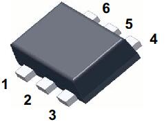
6
5
4
1
2
S1
1
6
D1
G1
2
5
G2
D2
3
4
S2
3
Absolute Maxim um Ratings
Sym bol
o
TA=25 C unl
essotherwi
se noted
Param eter
Ratings
Units
VDSS
Drai
n-Source Vol
tage
20
V
VGSS
Gate-Source Vol
tage
V
ID
Drai
n Current – Conti
nuous
– Pul
sed
Power Di
ssi
pati
on (Steady State)
r 12
600
1000
625
446
–55 to +150
PD
(Note 1a)
(Note 1a)
(Note 1b)
TJ,TSTG
Operati
ng and Storage Juncti
on Temperature
Range
mA
mW
qC
Therm alCharacteristics
RTJA
ThermalResi
stance,Juncti
on-to-Ambi
ent (Note 1a)
200
RTJA
ThermalResi
stance,Juncti
on-to-Ambi
ent (Note 1b)
280
qC/W
Package Marking and Ordering Inform ation
Device Marking
C
2007 Fai
rchi
l
d Semi
conductor Corporati
on
FDY3000NZ Rev B
Device
FDY3000NZ
ReelSize
7’
’
Tape width
8 mm
Quantity
3000 uni
ts
www.fai
rchi
l
dsemi
.com
FDY3000NZ DualN-Channel2.5V Specified PowerTrench MOSFET
January 2007
�Symbol
TA = 25°C unless otherwise noted
Parameter
Test Conditions
Min
Typ Max
Units
Off Characteristics
BVDSS
'BVDSS
���'TJ
IDSS
IGSS
Drain–Source Breakdown
Voltage
Breakdown Voltage Temperature
Coefficient
Zero Gate Voltage Drain Current
Gate–Body Leakage,
On Characteristics
VGS = 0 V,
ID = 250 PA
20
V
14
ID = 250 PA, Referenced to 25qC
VDS = 16 V,
VGS = 0 V
VGS = r 12 V, VDS = 0 V
VGS = r 4.5 V, VDS = 0 V
mV/qC
1
r 10
r1
PA
PA
PA
1.0
–3
1.3
V
mV/qC
0.25
0.37
0.73
0.35
1.8
0.70
0.85
1.25
1.00
:
(Note 2)
VGS(th)
'VGS(th)
���'TJ
RDS(on)
Gate Threshold Voltage
Gate Threshold Voltage
Temperature Coefficient
Static Drain–Source
On–Resistance
gFS
Forward Transconductance
VDS = VGS,
ID = 250 PA
ID = 250 PA, Referenced to 25qC
VGS = 4.5 V,
ID = 600 mA
VGS = 2.5 V,
ID = 500 mA
VGS = 1.8 V,
ID = 150 mA
VGS = 4.5 V, ID=600mA, TJ = 125qC
VDS = 5 V,
ID = 600 mA
0.6
S
Dynamic Characteristics
Ciss
Input Capacitance
Coss
Output Capacitance
Crss
Reverse Transfer Capacitance
Switching Characteristics
td(on)
Turn–On Delay Time
tr
Turn–On Rise Time
td(off)
Turn–Off Delay Time
tf
Turn–Off Fall Time
Qg
Total Gate Charge
Qgs
Gate–Source Charge
Qgd
Gate–Drain Charge
VDS = 10 V,
f = 1.0 MHz
V GS = 0 V,
60
pF
20
pF
10
pF
(Note 2)
VDD = 10 V,
VGS = 4.5 V,
VDS = 10 V,
VGS = 4.5 V
ID = 1 A,
RGEN = 6 :
ID = 600 mA,
6
12
ns
8
16
ns
8
16
ns
2.4
4.8
ns
0.8
1.1
nC
0.16
nC
0.26
nC
Drain–Source Diode Characteristics and Maximum Ratings
VSD
trr
Drain–Source Diode Forward
Voltage
Diode Reverse Recovery Time
Qrr
Diode Reverse Recovery Charge
VGS = 0 V,
IS = 150 mA
IF = 600 mA,
dIF/dt = 100 A/µs
(Note 2)
0.7
1.2
V
8
nS
1
nC
Notes:
unction-to-case and case-to-ambient thermal resistance where the case thermal reference is defined as the solder mounting surface of
1. RTJA is the sum of the j
the drain pins. RTJC is guaranteed by design while RTCA is determined by the user'
s board design
a)
200°C/W when
2
mounted on a 1in pad
of 2 oz copper
b) 280°C/W when mounted on a
minimum pad of 2 oz copper
Scale 1 :1 on letter size paper
2. Pulse Test:Pulse Width < 300Ps,
Duty Cycle < 2.0%
3. The diode connected between the gate
and source serves only as protection
againts ESD. No gate overvoltage
rating is implied.
FDY3000NZ Rev B
www.fairchildsemi.com
FDY3000NZ Dual N-Channel 2.5V Specified PowerTrench MOSFET
Electrical Characteristics
�1
2.6
3.0V
2.5V
RDS(ON),NORMALIZED
DRAIN-SOURCE ON-RESISTANCE
VGS = 4.5V
ID,DRAIN CURRENT (A)
3.5V
0.8
2.0V
0.6
0.4
0.2
2.4
VGS = 2.0V
2.2
2
1.8
1.6
2.5V
1.4
3.0V
1.2
3.5V
4.5V
1
0.8
0
0
0.25
0.5
0.75
0
1
0.2
0.4
Figure 1. On-Region Characteristics.
1
1
ID = 600mA
VGS = 4.5V
ID = 300mA
RDS(ON),ON-RESISTANCE (OHM)
RDS(ON),NORMALIZED
DRAIN-SOURCE ON-RESISTANCE
0.8
Figure 2. On-Resistance Variation with
Drain Current and Gate Voltage.
1.6
1.4
1.2
1
0.8
0.6
-50
-25
0
25
50
75
100
125
0.9
0.8
0.7
0.6
TA = 125oC
0.5
0.4
TA = 25oC
0.3
0.2
150
1
2
o
TJ,JUNCTION TEMPERATURE ( C)
3
4
5
VGS,GATE TO SOURCE VOLTAGE (V)
Figure 3. On-Resistance Variation with
Temperature.
Figure 4. On-Resistance Variation with
Gate-to-Source Voltage.
1
IS,REVERSE DRAIN CURRENT (A)
1
VDS = 5V
ID,DRAIN CURRENT (A)
0.6
ID,DRAIN CURRENT (A)
VDS,DRAIN-SOURCE VOLTAGE (V)
0.8
0.6
0.4
TA = 125oC
0.2
25oC
-55oC
VGS = 0V
0.1
TA = 125oC
0.01
25oC
-55oC
0.001
0.0001
0
0.5
1
1.5
2
VGS,GATE TO SOURCE VOLTAGE (V)
Figure 5. Transfer Characteristics.
FDY3000NZ Rev B
2.5
0
0.2
0.4
0.6
0.8
1
1.2
VSD,BODY DIODE FORW ARD VOLTAGE (V)
Figure 6. Body Diode Forward Voltage Variation
with Source Current and Temperature.
www.fairchildsemi.com
FDY3000NZ Dual N-Channel 2.5V Specified PowerTrench MOSFET
Typical Characteristics
�100
ID = 600mA
f = 1MHz
VGS = 0 V
90
4
80
VDS = 5V
10V
3
CAPACITANCE (pF)
VGS, GATE-SOURCE VOLTAGE (V)
5
15V
2
1
Ciss
70
60
50
40
Coss
30
20
10
0
Crss
0
0
0.2
0.4
0.6
0.8
1
0
4
Qg, GATE CHARGE (nC)
Figure 7. Gate Charge Characteristics.
16
20
30
1ms
1s
10ms
100ms
10s
DC
VGS = 4.5V
SINGLE PULSE
RTJA = 280oC/W
0.1
P(pk), PEAK TRANSIENT POWER (W)
RDS(ON) LIMIT
1
TA = 25oC
0.01
0.1
1
10
100
SINGLE PULSE
RTJA = 280°C/W
TA = 25°C
25
20
15
10
5
0
0.0001
0.001
0.01
0.1
1
10
100
1000
t1, TIME (sec)
VDS, DRAIN-SOURCE VOLTAGE (V)
Figure 9. Maximum Safe Operating Area.
r(t), NORMALIZED EFFECTIVE TRANSIENT
THERMAL RESISTANCE
12
Figure 8. Capacitance Characteristics.
10
ID, DRAIN CURRENT (A)
8
VDS, DRAIN TO SOURCE VOLTAGE (V)
Figure 10. Single Pulse Maximum
Power Dissipation.
1
D = 0.5
RTJA(t) = r(t) *RTJA
RTJA =280 °C/W
0.2
0.1
P(pk)
0.1
t1
0.05
t2
TJ - TA = P *RTJA(t)
Duty Cycle, D = t1 / t2
0.02
0.01
SINGLE PULSE
0.01
0.0001
0.001
0.01
0.1
1
10
100
1000
t1, TIME (sec)
Figure 11. Transient Thermal Response Curve.
Thermal characterization performed using the conditions described in Note 1b.
Transient thermal response will change depending on the circuit board design.
FDY3000NZ Rev B
www.fairchildsemi.com
FDY3000NZ Dual N-Channel 2.5V Specified PowerTrench MOSFET
Typical Characteristics
�SOT−563
CASE 419BH
ISSUE O
1.70
1.50
A
6
B
4
1.30
1.10
1.42
1.70
1.50
1
0.1 C B A
3
0.20
0.30
0.50
0.50
0.50
LAND PATTERN
RECOMMENDATION
TOP VIEW
0.60
0.50
0.72
C
SEATING PLANE
0.20
0.08
0.05 C
0.10
C
0.00
NOTES: UNLESS OTHERWISE SPECIFIED.
C
0.30
0.10
0.46
0.20
BOTTOM VIEW
A. REFERENCE TO JEDEC MO293.
B. ALL DIMENSIONS ARE IN MILLIMETERS.
C
DOES NOT COMPLY JEDEC STANDARD VALUE.
D. DIMENSIONS ARE EXCLUSIVE OF BURRS,
MOLD FLASH AND TIE BAR PROTRUSION.
E. DIMENSION AND TOLERANCE AS PER ASME
Y14.5−2009.
F. LANDPATTERN RECOMMENDATION GENERATED
WITH IPC LANDPATTERN GENERATOR
0.31
0.15
0.10 M C A B
0.05 M C
�ON Semiconductor and
are trademarks of Semiconductor Components Industries, LLC dba ON Semiconductor or its subsidiaries in the United States and/or other countries.
ON Semiconductor owns the rights to a number of patents, trademarks, copyrights, trade secrets, and other intellectual property. A listing of ON Semiconductor’s product/patent
coverage may be accessed at www.onsemi.com/site/pdf/Patent−Marking.pdf. ON Semiconductor reserves the right to make changes without further notice to any products herein.
ON Semiconductor makes no warranty, representation or guarantee regarding the suitability of its products for any particular purpose, nor does ON Semiconductor assume any liability
arising out of the application or use of any product or circuit, and specifically disclaims any and all liability, including without limitation special, consequential or incidental damages.
Buyer is responsible for its products and applications using ON Semiconductor products, including compliance with all laws, regulations and safety requirements or standards,
regardless of any support or applications information provided by ON Semiconductor. “Typical” parameters which may be provided in ON Semiconductor data sheets and/or
specifications can and do vary in different applications and actual performance may vary over time. All operating parameters, including “Typicals” must be validated for each customer
application by customer’s technical experts. ON Semiconductor does not convey any license under its patent rights nor the rights of others. ON Semiconductor products are not
designed, intended, or authorized for use as a critical component in life support systems or any FDA Class 3 medical devices or medical devices with a same or similar classification
in a foreign jurisdiction or any devices intended for implantation in the human body. Should Buyer purchase or use ON Semiconductor products for any such unintended or unauthorized
application, Buyer shall indemnify and hold ON Semiconductor and its officers, employees, subsidiaries, affiliates, and distributors harmless against all claims, costs, damages, and
expenses, and reasonable attorney fees arising out of, directly or indirectly, any claim of personal injury or death associated with such unintended or unauthorized use, even if such
claim alleges that ON Semiconductor was negligent regarding the design or manufacture of the part. ON Semiconductor is an Equal Opportunity/Affirmative Action Employer. This
literature is subject to all applicable copyright laws and is not for resale in any manner.
PUBLICATION ORDERING INFORMATION
LITERATURE FULFILLMENT:
Literature Distribution Center for ON Semiconductor
19521 E. 32nd Pkwy, Aurora, Colorado 80011 USA
Phone: 303−675−2175 or 800−344−3860 Toll Free USA/Canada
Fax: 303−675−2176 or 800−344−3867 Toll Free USA/Canada
Email: orderlit@onsemi.com
© Semiconductor Components Industries, LLC
N. American Technical Support: 800−282−9855 Toll Free
USA/Canada
Europe, Middle East and Africa Technical Support:
Phone: 421 33 790 2910
Japan Customer Focus Center
Phone: 81−3−5817−1050
www.onsemi.com
1
ON Semiconductor Website: www.onsemi.com
Order Literature: http://www.onsemi.com/orderlit
For additional information, please contact your local
Sales Representative
www.onsemi.com
�