FDZ4010
Integrated Load Switch
Features
General Description
The FDZ4010 is a 10 mA high side Pch MOSFET switch that can
be controlled by two enable signals. It is an AND function switch
activated by asserting both enable signals high. Input voltage
range operates from 2 V to 5 V to align with the requirement of
portable devices power requirement. FDZ4010 is uniquely
designed for optimized low power dissipation and precise driver
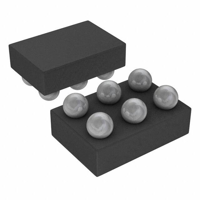
requirement. FDZ4010 comes in a tiny 0.8 mm X 1.2 mm
WLCSP, 6 bumps, with 0.4 mm pitch.
Input Voltage Range from 2 V to 5 V
10 mA output current
UItra Thin and Small Package WL-CSP
0.8 X 1.2 mm2, Height 0.5 mm
RoHS Compliant
Application
Smart Phone / Table Accessory
TOP View
BOTTOM View
6 Balls, 0.8 X 1.2 mm2 WL-CSP
Package Marking and Ordering Information
Part
Number
Device Marking
Ball Pitch
Package
Reel Size
Tape Width
Quantity
FDZ4010
Z5
0.4 mm
0.8 mm x 1.2 mm
WL-CSP, 6 Bumps
7 ’’
8 mm
3000
For Fairchild’s definition of Eco Status, please visit: http://www.fairchildsemi.com/company/green/rohs_green.html
©2013 Fairchild Semiconductor Corporation
FDZ4010 Rev.C4
1
www.fairchildsemi.com
FDZ4010
July 2013
�FDZ4010
Application Diagram
VIN
IN
EN1
EN2
OUT
FDZ4010
VOUT
GND
Figure 1. Typical Application
Block Diagram
IN
OUT
Output
Discharge
EN1
CONTROL
BLOCK
EN2
R EN
RE N
GND
Figure 2. Functional Block Diagram
Truth Table
VIN (2 V to 5 V)
YES
YES
EN1
HIGH
LOW
EN2
HIGH
LOW
PCH MOSFET Status
ON
OFF
VOUT Status
VIN
LOW
YES
YES
HIGH
LOW
LOW
HIGH
OFF
OFF
LOW
LOW
Table 1. Truth Table for OUT Status
©2013 Fairchild Semiconductor Corporation
FDZ4010 Rev.C4
2
www.fairchildsemi.com
�FDZ4010
Pin Configuration
A
A1
A2
A2
A1
A
B
B1
B2
B2
B1
B
C
C1
C2
C2
C1
C
1
2
2
1
Top View
Bottom View
Figure 3. Pin Assignments
Pin Definitions
Pin #
A1
Name
IN
A2
OUT
B1, C1
B2
C2
GND
EN1
EN2
Description
Input of the Pch MOSFET Switch
Output of the Pch MOSFET Switch. Internally, this pin is pulled down through an output discharge
FET to Ground when EN pins are low and VIN is present.
Ground
ON/OFF control input, Active High.
ON/OFF control input, Active High.
©2013 Fairchild Semiconductor Corporation
FDZ4010 Rev.C4
3
www.fairchildsemi.com
�Characteristics
Min.
-0.3
-0.3
VIN, VOUT to GND
VEN1,VEN2 to GND
Continuous Output Current
Junction Temperature (TJ)
Storage Temperature Range (TSTG)
Thermal Resistance, Junction to Ambient (
Electrostatic Discharge
-65
JA)
(Note 1b)
Human Body Model, ANSI/ESDA/
JEDEC JS-001-2012
Charged Device Model, JESD22C101
Max.
6
6
Unit
V
V
20
150
150
312
mA
o
C
o
C
°C/W
5
kV
2
Recommended Operating Conditions
Characteristics
IN Voltage
OUT Current, VIN = 3.3 V ,
VEN1 = VEN2 = 3.3 V
EN1, EN2 Voltage
Operating Temperature Range
Symbol
VIN
Min.
2
IOUT
VEN1 ,VEN2
Max.
5
Unit
V
10
mA
5
-40
85
V
oC
Notes:
1. R JA is the sum of the junction-to-case and case-to-ambient thermal resistance where the case thermal reference is defined as the solder mounting
suface of the drain pins. R JC is guaranteed by design while R CA is determined by the user’s board design.
a. 115 °C/W when mounted on
a 1 in2 pad of 2 oz copper.
b. 312 °C/W when mounted on a
minimum pad of 2 oz copper.
OUTS
OUTF
INS
INF
OUTS
OUTF
INS
INF
©2013 Fairchild Semiconductor Corporation
FDZ4010 Rev.C4
4
www.fairchildsemi.com
FDZ4010
Absolute Maximum Ratings
�Symbol
Parameter
VIH
Input High Voltage, EN1, EN2
VIH
Input High Voltage, EN1, EN2
VIL
Input Low Voltage, EN1, EN2
REN
Pull Down Resistance at EN1, EN2
CEN
Input Capacitance of EN1, EN2
RDS(ON)
On-Resistance of Pch MOSFET
IQ
Quiescent Current
ISD
Shutdown Current
ton
tr
toff
ROUT
Pull Down Resistance at OUT Pin
Turn-On Time
Turn-On Rise Time
Turn-Off Time
tf
Turn-Off Fall Time
Test Conditions
VIN = 2.5 V to 5 V and across
temperature range
VIN = 2 V and across temperature range
VIN = 2 V to 5 V and across temperature
range
VEN1 = VEN2 = 1 V and across
temperature range
f = 1 MHz and across temperature range
(Note 2)
IOUT = 10 mA, VIN = 2 V to 5 V
VIN = 5 V, VEN1 = VEN2 = 5 V,
VOUT floating (IOUT = 0),
Across temperature range
VIN = 3.3 V, VEN1 = VEN2 = 0 V,
VOUT floating (IOUT = 0),
Across temperature range
VIN = 3.3 V,
VEN1 = 825 mV & VEN2 = 425 mV,
VEN1 = 425 mV & VEN2 = 825 mV,
VOUT floating (IOUT = 0),
Across temperature range
VEN1 = VEN2 = 0 V
Load Impedance,
VIN = 3.3 V,
CL = 50 pF, RL = 500
VEN1 = VEN2 = 0 V to 2.3 V,
(500 ns rise time)
Min
Typ
Max
Units
1.375
V
1.525
V
0.95
70
100
V
130
k
10
pF
1.5
1
500
A
1
A
10
A
1.3
1
0.95
2
2
k
s
s
s
s
Notes:
2. Guaranteed by characterization and design
Figure 4. Timing Diagram
©2013 Fairchild Semiconductor Corporation
FDZ4010 Rev.C4
5
www.fairchildsemi.com
FDZ4010
Electrical Characteristics VIN = 2 V to 5 V, TJ = 25 oC , unless otherwise noted
�FDZ4010
Typical Characteristics (Continued)
350
400
VEN1 = VEN2 = VIN
VIN = 5.0 V
350 V
= Floating
OUT
SUPPLY CURRENT ( A)
SUPPLY CURRENT ( A)
VEN1 = VEN2 = 5.0 V
300
250
200
-50
-25
0
25
50
75
300
250
200
150
100
2.0
100
TA = 25 oC
2.5
3.0
o
Figure 5. Quiescent Current vs Temperature
SHUTDOWN CURRENT ( A)
SHUTDOWN CURRENT (nA)
VEN1 = 0 V
VEN2 = 0 V
VIN = 3.3 V
40
20
-25
0
25
50
75
VEN2 = 0 V
6
TA = 25 oC
4
2
2.0
100
o
2.5
3.0
TJ, JUNCTION TEMPERATURE ( C)
4.0
4.5
5.0
Figure 8. Shutdown Current vs Supply Voltage
4
VEN1 = 425 mV
VEN1 = 825 mV
VEN2 = 825 mV
SHUTDOWN CURRENT ( A)
SHUTDOWN CURRENT ( A)
3.5
SUPPLY VOLTAGE (V)
Figure 7. Shutdown Current vs Temperature
VIN = 3.3 V
3
2
1
-50
5.0
8
VEN1 = 0 V
4
4.5
Figure 6. Quiescent Current vs Supply Voltage
80
0
-50
4.0
SUPPLY VOLTAGE (V)
TJ, JUNCTION TEMPERATURE ( C)
60
3.5
-25
0
25
50
75
3
VIN = 3.3 V
2
1
-50
100
-25
0
25
50
75
100
TJ, JUNCTION TEMPERATURE (oC)
TJ, JUNCTION TEMPERATURE (oC)
Figure 9. Shutdown Current vs Temperature
©2013 Fairchild Semiconductor Corporation
FDZ4010 Rev.C4
VEN2 = 425 mV
Figure 10. Shutdown Current vs Temperature
6
www.fairchildsemi.com
�FDZ4010
Typical Characteristics (Continued)
1.4
VIN = VEN2 = 3.3 V
EN1 INPUT LOGIC VOLTAGE (V)
EN1 INPUT LOGIC VOLTAGE (V)
1.4
1.3
1.2
VIL
VIH
1.1
1.0
-50
-25
0
25
50
75
1.3
VIN = VEN2
1.2
VIL
VIH
1.1
1.0
2.0
100
TA = 25 oC
2.5
o
TJ, JUNCTION TEMPERATURE ( C)
Figure 11. EN1 Logic Voltage vs Temperature
1.4
VIN = VEN1 = 3.3 V
1.3
1.2
VIL
VIH
1.1
1.0
-50
-25
0
25
50
3.5
75
VIN = VEN1
1.2
VIL
VIH
1.1
1.0
2.0
100
2.5
3.0
3.5
4.0
4.5
5.0
SUPPLY VOLTAGE (V)
Figure 13. EN2 Logic Voltage vs Temperature
Figure 14. EN2 Logic Voltage vs Supply Voltage (VIN)
400
500
VEN1 = VEN2 = 3.3 V
VEN1 = VEN2 = VIN
STATIC DRAIN TO SOURCE
ON RESISTANCE (m )
VIN = 3.3 V
STATIC DRAIN TO SOURCE
ON RESISTANCE (m )
5.0
1.3
TJ, JUNCTION TEMPERATURE ( C)
IOUT = 10 mA
300
250
-50
4.5
TA = 25 oC
o
350
4.0
Figure 12. EN1 Logic Voltage vs Supply Voltage (V IN)
EN2 INPUT LOGIC VOLTAGE (V)
EN2 INPUT LOGIC VOLTAGE (V)
1.4
3.0
SUPPLY VOLTAGE (V)
-25
0
25
50
75
TJ, JUNCTION TEMPERATURE ( C)
400
350
300
2.5
3.0
3.5
4.0
4.5
5.0
SUPPLY VOLTAGE (V)
Figure15. Static Drain to Source ON
Resistance vs Temperature
©2013 Fairchild Semiconductor Corporation
FDZ4010 Rev.C4
TA = 25 oC
250
2.0
100
o
IOUT = 10 mA
450
Figure 16. Static Drain to Source ON
Resistance vs Supply Voltage
7
www.fairchildsemi.com
�FDZ4010
Typical Characteristics (Continued)
5.8
6.0
FUNC: Cp-Rp
FREQ: 1 MHz
LEVEL: 100 mV
EN2 CAPACITANCE (pF)
EN1 CAPACITANCE (pF)
6.0
5.6
5.4
5.2
5.0
-50
-25
0
25
50
75
5.6
5.4
5.2
5.0
-50
100
TJ, JUNCTION TEMPERATURE (oC)
-25
0
25
50
75
100
TJ, JUNCTION TEMPERATURE (oC)
Figure 17. EN1 Capacitance vs Temperature
©2013 Fairchild Semiconductor Corporation
FDZ4010 Rev.C4
FUNC: Cp-Rp
FREQ: 1 MHz
LEVEL: 100 mV
5.8
Figure 18. EN2 Capacitance vs Temperature
8
www.fairchildsemi.com
�FDZ4010
Typical Characteristics (Continued)
VEN1
VIN
VOUT
Figure 19. Turn-On Time (VIN = 3.3 V, VEN2 = 2.3 V,
timescale = 40 us/div)
VEN1= 0 to 2.3 V, COUT = 50 pF, RL= 500
VEN1
VOUT
VIN
Figure 20. Turn-Off Time (VIN = 3.3 V, VEN2 = 2.3 V,
timescale = 40 us/div)
VEN1= 2.3 to 0 V, COUT = 50 pF, RL= 500
©2013 Fairchild Semiconductor Corporation
FDZ4010 Rev.C4
9
www.fairchildsemi.com
�FDZ4010
Typical Characteristics (Continued)
VIN
Figure 21. VIN Ramp Up and Down (VIN = 0 to 4.8 V (6100 V/sec),
timescale = 400 us/div)
EN1 and EN2 are floating(Internally GND), COUT = 50 pF, RL= 500
VIN
Figure 22. VIN Ramp Up and Down (EN1 = EN2 = VIN = 0 to 4.8 V (6100 V/sec),
COUT = 50 pF, RL= 500
©2013 Fairchild Semiconductor Corporation
FDZ4010 Rev.C4
, timescale = 400 us/div)
10
www.fairchildsemi.com
�FDZ4010
Application Information
IN
V IN
OF F/ ON
2V ~ 5V
C IN =
0.1 uF
OF F/O N
EN1
EN2
FDZ4010
V OU T
O UT
G ND
CL=
50 pF
RL=
500O
(Optional)
Figure 23. Typical Application Circuit
Input Voltage
Input Voltage (VIN) is set from 2 V to 5 V.
Input Capacitor
To prevent the input voltage being pulled below the minimum operating voltage, a reservoir capacitor can be connected from IN to
GND. 0.1 F ceramic type is suitable.
Enable/Shutdown Operation
To turn on the switch, both the EN pins need to be asserted high. To ensure proper operation, Enable signals must be able to swing
above and below the specified turn-on/off voltage threshold described in the Electrical Charateristics table under VIL and VIH for the
selected input voltage.
Power up Sequence
Turn on input voltage (VIN) within range from 2 V to 5 V then turn on EN1 or/and EN2 signal. VOUT status changed by EN1 or/and EN2
signal input and defined the status in Table 1 Truth Table.
©2013 Fairchild Semiconductor Corporation
FDZ4010 Rev.C4
11
www.fairchildsemi.com
�FDZ4010
Dimensional Outline and Pad Layout
Product-Specific Dimensions
Product
D
E
X
Y
FDZ4010
1.16 mm
0.76 mm
0.18 mm
0.18 mm
©2013 Fairchild Semiconductor Corporation
FDZ4010 Rev.C4
12
www.fairchildsemi.com
�FDZ4010
TRADEMARKS
The following includes registered and unregistered trademarks and service marks, owned by Fairchild Semiconductor and/or its global subsidiaries, and is not
intended to be an exhaustive list of all such trademarks.
2Cool™
Sync-Lock™
FPS™
®
AccuPower™
F-PFS™
®*
®
®
®
FRFET
AX-CAP *
PowerTrench
SM
Global Power Resource
PowerXS™
BitSiC™
TinyBoost™
Green Bridge™
Build it Now™
Programmable Active Droop™
TinyBuck™
CorePLUS™
Green FPS™
QFET®
TinyCalc™
CorePOWER™
QS™
Green FPS™ e-Series™
TinyLogic®
Gmax™
CROSSVOLT™
Quiet Series™
TINYOPTO™
GTO™
CTL™
RapidConfigure™
TinyPower™
IntelliMAX™
Current Transfer Logic™
™
TinyPWM™
®
ISOPLANAR™
DEUXPEED
TinyWire™
Marking Small Speakers Sound Louder Saving our world, 1mW/W/kW at a time™
Dual Cool™
TranSiC®
and Better™
EcoSPARK®
SignalWise™
TriFault Detect™
EfficentMax™
MegaBuck™
SmartMax™
TRUECURRENT®*
MICROCOUPLER™
SMART START™
ESBC™
SerDes™
MicroFET™
Solutions for Your Success™
®
MicroPak™
SPM®
MicroPak2™
STEALTH™
Fairchild®
UHC®
MillerDrive™
SuperFET®
Fairchild Semiconductor®
Ultra FRFET™
SuperSOT™-3
MotionMax™
FACT Quiet Series™
UniFET™
mWSaver™
SuperSOT™-6
FACT®
VCX™
OptoHiT™
SuperSOT™-8
FAST®
®
®
VisualMax™
OPTOLOGIC
SupreMOS
FastvCore™
®
VoltagePlus™
OPTOPLANAR
SyncFET™
FETBench™
XS™
tm
*Trademarks of System General Corporation, used under license by Fairchild Semiconductor.
DISCLAIMER
FAIRCHILD SEMICONDUCTOR RESERVES THE RIGHT TO MAKE CHANGES WITHOUT FURTHER NOTICE TO ANY PRODUCTS HEREIN TO IMPROVE
RELIABILITY, FUNCTION, OR DESIGN. FAIRCHILD DOES NOT ASSUME ANY LIABILITY ARISING OUT OF THE APPLICATION OR USE OF ANY
PRODUCT OR CIRCUIT DESCRIBED HEREIN; NEITHER DOES IT CONVEY ANY LICENSE UNDER ITS PATENT RIGHTS, NOR THE RIGHTS OF OTHERS.
THESE SPECIFICATIONS DO NOT EXPAND THE TERMS OF FAIRCHILD’S WORLDWIDE TERMS AND CONDITIONS, SPECIFICALLY THE WARRANTY
THEREIN, WHICH COVERS THESE PRODUCTS.
LIFE SUPPORT POLICY
FAIRCHILD’S PRODUCTS ARE NOT AUTHORIZED FOR USE AS CRITICAL COMPONENTS IN LIFE SUPPORT DEVICES OR SYSTEMS WITHOUT THE
EXPRESS WRITTEN APPROVAL OF FAIRCHILD SEMICONDUCTOR CORPORATION.
As used here in:
1. Life support devices or systems are devices or systems which, (a) are
intended for surgical implant into the body or (b) support or sustain life,
and (c) whose failure to perform when properly used in accordance with
instructions for use provided in the labeling, can be reasonably
expected to result in a significant injury of the user.
2.
A critical component in any component of a life support, device, or
system whose failure to perform can be reasonably expected to cause
the failure of the life support device or system, or to affect its safety or
effectiveness.
ANTI-COUNTERFEITING POLICY
Fairchild Semiconductor Corporation’s Anti-Counterfeiting Policy. Fairchild’s Anti-Counterfeiting Policy is also stated on our external website,
www.Fairchildsemi.com, under Sales Support.
Counterfeiting of semiconductor parts is a growing problem in the industry. All manufactures of semiconductor products are experiencing counterfeiting of their
parts. Customers who inadvertently purchase counterfeit parts experience many problems such as loss of brand reputation, substandard performance, failed
application, and increased cost of production and manufacturing delays. Fairchild is taking strong measures to protect ourselves and our customers from the
proliferation of counterfeit parts. Fairchild strongly encourages customers to purchase Fairchild parts either directly from Fairchild or from Authorized Fairchild
Distributors who are listed by country on our web page cited above. Products customers buy either from Fairchild directly or from Authorized Fairchild
Distributors are genuine parts, have full traceability, meet Fairchild’s quality standards for handing and storage and provide access to Fairchild’s full range of
up-to-date technical and product information. Fairchild and our Authorized Distributors will stand behind all warranties and will appropriately address and
warranty issues that may arise. Fairchild will not provide any warranty coverage or other assistance for parts bought from Unauthorized Sources. Fairchild is
committed to combat this global problem and encourage our customers to do their part in stopping this practice by buying direct or from authorized distributors.
PRODUCT STATUS DEFINITIONS
Definition of Terms
Datasheet Identification
Product Status
Definition
Advance Information
Formative / In Design
Datasheet contains the design specifications for product development. Specifications
may change in any manner without notice.
Preliminary
First Production
Datasheet contains preliminary data; supplementary data will be published at a later
date. Fairchild Semiconductor reserves the right to make changes at any time without
notice to improve design.
No Identification Needed
Full Production
Datasheet contains final specifications. Fairchild Semiconductor reserves the right to
make changes at any time without notice to improve the design.
Obsolete
Not In Production
Datasheet contains specifications on a product that is discontinued by Fairchild
Semiconductor. The datasheet is for reference information only.
Rev. I64
©2013 Fairchild Semiconductor Corporation
FDZ4010 Rev.C4
13
www.fairchildsemi.com
�