Is Now Part of
To learn more about ON Semiconductor, please visit our website at
www.onsemi.com
Please note: As part of the Fairchild Semiconductor integration, some of the Fairchild orderable part numbers
will need to change in order to meet ON Semiconductor’s system requirements. Since the ON Semiconductor
product management systems do not have the ability to manage part nomenclature that utilizes an underscore
(_), the underscore (_) in the Fairchild part numbers will be changed to a dash (-). This document may contain
device numbers with an underscore (_). Please check the ON Semiconductor website to verify the updated
device numbers. The most current and up-to-date ordering information can be found at www.onsemi.com. Please
email any questions regarding the system integration to Fairchild_questions@onsemi.com.
ON Semiconductor and the ON Semiconductor logo are trademarks of Semiconductor Components Industries, LLC dba ON Semiconductor or its subsidiaries in the United States and/or other countries. ON Semiconductor owns the rights to a number
of patents, trademarks, copyrights, trade secrets, and other intellectual property. A listing of ON Semiconductor’s product/patent coverage may be accessed at www.onsemi.com/site/pdf/Patent-Marking.pdf. ON Semiconductor reserves the right
to make changes without further notice to any products herein. ON Semiconductor makes no warranty, representation or guarantee regarding the suitability of its products for any particular purpose, nor does ON Semiconductor assume any liability
arising out of the application or use of any product or circuit, and specifically disclaims any and all liability, including without limitation special, consequential or incidental damages. Buyer is responsible for its products and applications using ON
Semiconductor products, including compliance with all laws, regulations and safety requirements or standards, regardless of any support or applications information provided by ON Semiconductor. “Typical” parameters which may be provided in ON
Semiconductor data sheets and/or specifications can and do vary in different applications and actual performance may vary over time. All operating parameters, including “Typicals” must be validated for each customer application by customer’s
technical experts. ON Semiconductor does not convey any license under its patent rights nor the rights of others. ON Semiconductor products are not designed, intended, or authorized for use as a critical component in life support systems or any FDA
Class 3 medical devices or medical devices with a same or similar classification in a foreign jurisdiction or any devices intended for implantation in the human body. Should Buyer purchase or use ON Semiconductor products for any such unintended
or unauthorized application, Buyer shall indemnify and hold ON Semiconductor and its officers, employees, subsidiaries, affiliates, and distributors harmless against all claims, costs, damages, and expenses, and reasonable attorney fees arising out
of, directly or indirectly, any claim of personal injury or death associated with such unintended or unauthorized use, even if such claim alleges that ON Semiconductor was negligent regarding the design or manufacture of the part. ON Semiconductor
is an Equal Opportunity/Affirmative Action Employer. This literature is subject to all applicable copyright laws and is not for resale in any manner.
�FFP15S60S
15 A, 600 V, STEALTH™ II Diode
Features
Description
• Stealth Recovery Trr = 35 ns (@ IF = 15 A)
The FFP15S60S is a STEALTH™ II diode with soft recovery characteristics. It is silicon nitride passivated ion-implanted epitaxial
planar construction. This device is intended for use as freewheeling of boost diode in switching power supplies and other power
swithching applications. Their low stored charge and hyperfast
soft recovery minimize ringing and electrical noise in many power
switching circuits reducing power loss in the switching transistors.
• Max Forward Voltage, VF = 2.6 V (@ TC = 25oC)
• 600 V Reverse Voltage and High Reliability
• Improved dv/dt Capability
• RoHS compliant
Applications
• General Purpose
• SMPS, Power Switching Circuits
• Boost Diode in Continuous Mode Power Factor Corrections
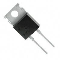
TO-220-2L
1. Cathode
2. Anode
1. Cathode
2. Anode
Absolute Maximum Ratings TC = 25oC unless otherwise noted
Symbol
VRRM
Peak Repetitive Reverse Voltage
Parameter
FFP15S60S
600
Unit
V
VRWM
VR
Working Peak Reverse Voltage
600
V
DC Blocking Voltage
600
IF(AV)
Average Rectified Forward Current
V
15
IFSM
Non-repetitive Peak Surge Current
60Hz Single Half-Sine Wave
A
150
A
TJ, TSTG
Operating and Storage Temperature Range
@ TC = 123oC
o
-65 to +175
C
Thermal Characteristics
Symbol
RθJC
Parameter
FFP15S60S
Maximum Thermal Resistance, Junction to Case
1.3
Unit
o
C/W
Package Marking and Ordering Information
Part Number
Top Mark
Package
Packing Method
Reel Size
Tape Width
Quantity
FFP15S60STU
F15S60S
TO-220-2L
Tube
N/A
N/A
50
©2007 Fairchild Semiconductor Corporation
FFP15S60S Rev. 1.8
1
www.fairchildsemi.com
FFP15S60S — STEALTH™ II Diode
May 2015
�Symbol
Min.
Typ.
Max.
Unit
VF1
IF = 15 A
IF = 15 A
Parameter
TC = 25oC
TC = 125oC
-
2.1
1.6
2.6
-
V
IR 1
VR = 600 V
VR = 600 V
TC = 25oC
TC = 125oC
-
-
100
500
μA
trr
IF = 1A, di/dt = 100 A/μs, VR = 30 V
TC = 25oC
-
21
30
ns
trr
Irr
S factor
Qrr
IF = 15 A, di/dt = 200 A/μs, VR = 390 V
TC = 25oC
-
23
2.5
0.7
29
35
-
ns
A
-
55
4.3
1.1
118
-
nC
20
-
-
mJ
trr
Irr
S factor
Qrr
IF = 15 A, di/dt = 200 A/μs, VR = 390 V
WAVL
Avalanche Energy ( L = 40 mH)
TC =
125oC
nC
ns
A
Notes:
1: Pulse: Test Pulse width = 300μs, Duty Cycle = 2%
Test Circuit and Waveforms
Figure 1. Diode Reverse Recovery Test Circuit & Waveform
Figure 2. Unclamped Inductive Switching Test Circuit & Waveform
©2007 Fairchild Semiconductor Corporation
FFP15S60S Rev. 1.8
2
www.fairchildsemi.com
FFP15S60S — STEALTH™ II Diode
Electrical Characteristics TC = 25oC unless otherwise noted
�Figure 3. Typical Forward Voltage Drop
vs. Forward Current
Figure 4. Typical Reverse Current
vs. Reverse Voltage
100
70
o
10
o
Reverse Current, IR [μA]
Forward Current, IF [A]
TC = 125 C
o
TC = 75 C
o
TC = 25 C
1
TC = 125 C
10
o
TC =75 C
1
0.1
o
TC = 25 C
0.1
0
1
2
3
Forward Voltage, VF [V]
0.01
4
Figure 5. Typical Junction Capacitance
Typical Capacitance
at 0V = 180 pF
Capacitances, Cj [pF]
150
120
90
60
30
0.1
1
10
Reverse Voltage, VR [V]
500
o
600
IF = 15A
TC = 125 C
50
o
40
TC = 75 C
30
TC = 25 C
20
100
o
200
300
400
di/dt [A/μs]
500
600
Figure 8. Forward Current Derating Curve
50
6
Average Forward Current, IF(AV) [A]
7
Reverse Recovery Current, Irr [A]
200
300
400
Reverse Voltage, VR [V]
60
100
Figure 7. Typical Reverse Recovery
Current vs. di/dt
o
TC = 125 C
5
4
o
TC = 75 C
3
o
TC = 25 C
2
IF = 15A
1
100
100
Figure 6. Typical Reverse Recovery Time
vs. di/dt
Reverse Recovery Time, trr [ns]
180
10
200
300
400
500
30
20
3
DC
10
0
25
600
di/dt [A/μs]
©2007 Fairchild Semiconductor Corporation
FFP15S60S Rev. 1.8
40
50
75
100
125
o
Case temperature, TC [ C]
150
www.fairchildsemi.com
FFP15S60S — STEALTH™ II Diode
Typical Performance Characteristics
�4.09
3.50
0.36 M
10.67
9.65
A
B A M
B
3.43
2.54
8.89
6.86
1.40
0.51
7°
3°
6.86
5.84
16.51
14.22
9.40
8.38
5°
3°
1
2
5°
3°
16.15
15.75
13.40
12.19
6.35 MAX
0.60 MAX
C
1.65
1.25
1.91
14.73
13.60
0.61
0.33
2.54
2.92
2.03
1.02
0.38
5.08
5°
3°
0.36 M
C A B
5°
3°
4.80
4.30
NOTES:
A. PACKAGE REFERENCE: JEDEC TO220,ISSUE K,
VARIATION AC,DATED APRIL 2002.
B. ALL DIMENSIONS ARE IN MILLIMETERS.
C. DIMENSION AND TOLERANCE AS PER ASME
Y14.5-2009.
D. DIMENSIONS ARE EXCLUSIVE OF BURRS,
MOLD FLASH AND TIE BAR PROTRUSIONS.
E. DRAWING FILE NAME: TO220A02REV5
�ON Semiconductor and
are trademarks of Semiconductor Components Industries, LLC dba ON Semiconductor or its subsidiaries in the United States and/or other countries.
ON Semiconductor owns the rights to a number of patents, trademarks, copyrights, trade secrets, and other intellectual property. A listing of ON Semiconductor’s product/patent
coverage may be accessed at www.onsemi.com/site/pdf/Patent−Marking.pdf. ON Semiconductor reserves the right to make changes without further notice to any products herein.
ON Semiconductor makes no warranty, representation or guarantee regarding the suitability of its products for any particular purpose, nor does ON Semiconductor assume any liability
arising out of the application or use of any product or circuit, and specifically disclaims any and all liability, including without limitation special, consequential or incidental damages.
Buyer is responsible for its products and applications using ON Semiconductor products, including compliance with all laws, regulations and safety requirements or standards,
regardless of any support or applications information provided by ON Semiconductor. “Typical” parameters which may be provided in ON Semiconductor data sheets and/or
specifications can and do vary in different applications and actual performance may vary over time. All operating parameters, including “Typicals” must be validated for each customer
application by customer’s technical experts. ON Semiconductor does not convey any license under its patent rights nor the rights of others. ON Semiconductor products are not
designed, intended, or authorized for use as a critical component in life support systems or any FDA Class 3 medical devices or medical devices with a same or similar classification
in a foreign jurisdiction or any devices intended for implantation in the human body. Should Buyer purchase or use ON Semiconductor products for any such unintended or unauthorized
application, Buyer shall indemnify and hold ON Semiconductor and its officers, employees, subsidiaries, affiliates, and distributors harmless against all claims, costs, damages, and
expenses, and reasonable attorney fees arising out of, directly or indirectly, any claim of personal injury or death associated with such unintended or unauthorized use, even if such
claim alleges that ON Semiconductor was negligent regarding the design or manufacture of the part. ON Semiconductor is an Equal Opportunity/Affirmative Action Employer. This
literature is subject to all applicable copyright laws and is not for resale in any manner.
PUBLICATION ORDERING INFORMATION
LITERATURE FULFILLMENT:
Literature Distribution Center for ON Semiconductor
19521 E. 32nd Pkwy, Aurora, Colorado 80011 USA
Phone: 303−675−2175 or 800−344−3860 Toll Free USA/Canada
Fax: 303−675−2176 or 800−344−3867 Toll Free USA/Canada
Email: orderlit@onsemi.com
© Semiconductor Components Industries, LLC
N. American Technical Support: 800−282−9855 Toll Free
USA/Canada
Europe, Middle East and Africa Technical Support:
Phone: 421 33 790 2910
Japan Customer Focus Center
Phone: 81−3−5817−1050
www.onsemi.com
1
ON Semiconductor Website: www.onsemi.com
Order Literature: http://www.onsemi.com/orderlit
For additional information, please contact your local
Sales Representative
www.onsemi.com
�


 工商网监
湘ICP备2023018690号
工商网监
湘ICP备2023018690号
