ON Semiconductor
Is Now
To learn more about onsemi™, please visit our website at
www.onsemi.com
onsemi and and other names, marks, and brands are registered and/or common law trademarks of Semiconductor Components Industries, LLC dba “onsemi” or its affiliates and/or
subsidiaries in the United States and/or other countries. onsemi owns the rights to a number of patents, trademarks, copyrights, trade secrets, and other intellectual property. A listing of onsemi
product/patent coverage may be accessed at www.onsemi.com/site/pdf/Patent-Marking.pdf. onsemi reserves the right to make changes at any time to any products or information herein, without
notice. The information herein is provided “as-is” and onsemi makes no warranty, representation or guarantee regarding the accuracy of the information, product features, availability, functionality,
or suitability of its products for any particular purpose, nor does onsemi assume any liability arising out of the application or use of any product or circuit, and specifically disclaims any and all
liability, including without limitation special, consequential or incidental damages. Buyer is responsible for its products and applications using onsemi products, including compliance with all laws,
regulations and safety requirements or standards, regardless of any support or applications information provided by onsemi. “Typical” parameters which may be provided in onsemi data sheets and/
or specifications can and do vary in different applications and actual performance may vary over time. All operating parameters, including “Typicals” must be validated for each customer application
by customer’s technical experts. onsemi does not convey any license under any of its intellectual property rights nor the rights of others. onsemi products are not designed, intended, or authorized
for use as a critical component in life support systems or any FDA Class 3 medical devices or medical devices with a same or similar classification in a foreign jurisdiction or any devices intended for
implantation in the human body. Should Buyer purchase or use onsemi products for any such unintended or unauthorized application, Buyer shall indemnify and hold onsemi and its officers, employees,
subsidiaries, affiliates, and distributors harmless against all claims, costs, damages, and expenses, and reasonable attorney fees arising out of, directly or indirectly, any claim of personal injury or death
associated with such unintended or unauthorized use, even if such claim alleges that onsemi was negligent regarding the design or manufacture of the part. onsemi is an Equal Opportunity/Affirmative
Action Employer. This literature is subject to all applicable copyright laws and is not for resale in any manner. Other names and brands may be claimed as the property of others.
�20 A, 600 V, Ultrafast Dual Diode
Description
Features
The FFPF20UP60DN is a ultrafast dual diode with low forward
voltage drop. This device is intended for use as freewheeling and
clamping diodes in a variety of switching power supplies and
other power switching applications. It is specially suited for use in
switching power supplies and industrial application.
• Ultrafast Recovery trr = 70 ns (@ IF = 10 A)
• Max Forward Voltage, VF = 2.2 V (@ TC = 25°C)
• 600 V Reverse Voltage and High Reliability
• Avalanche Energy Rated
• RoHS Compliant
Applications
• General Purpose
• SMPS, Power Switching Circuits
• Boost Diode in Continuous Mode Power Factor Corrections
1
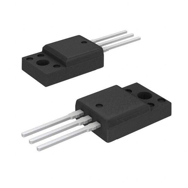
TO-220F
3
2
1. Anode 2. Cathode 3. Anode
1 2 3
Absolute Maximum Ratings TC = 25oC unless otherwise noted
Symbol
VRRM
Peak Repetitive Reverse Voltage
Parameter
Rating
600
Unit
V
VRWM
VR
Working Peak Reverse Voltage
600
V
DC Blocking Voltage
600
IF(AV)
Average Rectified Forward Current
V
10
IFSM
Non-repetitive Peak Surge Current
60Hz Single Half-Sine Wave
A
50
A
TJ, TSTG
Operating and Storage Temperature Range
@ TC = 103oC
o
-65 to +175
C
Thermal Characteristics
Symbol
RJC
Parameter
Max.
Maximum Thermal Resistance, Junction to Case
Unit
o
7
C/W
Package Marking and Ordering Information
Part Number
Top Mark
Package
Packing Method
Reel Size
Tape Width
Quantity
FFPF20UP60DNTU
FFPF20UP60DN
TO-220F
Tube
N/A
N/A
50
©2007 Semiconductor Components Industries, LLC.
October-2017,Rev. 3
Publication Order Number:
FFPF20UP60DN/D
FFPF20UP60DN — Ultrafast Dual Diode
FFPF20UP60DN
�Symbol
Min.
Typ.
Max.
Unit
V F1
IF = 10 A
IF = 10 A
Parameter
TC = 25oC
TC = 100oC
-
-
2.2
2.0
V
IR1
VR = 600 V
VR = 600 V
TC = 25oC
TC = 100oC
-
-
100
500
A
trr
IF = 10 A, diF/dt = 200 A/s, VR = 390 V
TC = 25oC
-
53
70
ns
trr
Irr
Qrr
IF = 1 A, diF/dt = 100 A/s, VR = 30 V
TC = 25oC
-
30
1.5
20
40
2
30
ns
A
nC
WAVL
Avalanche Energy ( L = 40 mH)
10
-
-
mJ
Notes:
1: Pulse: Test Pulse width = 300s, Duty Cycle = 2%
Test Circuit and Waveforms
Figure 1. Diode Reverse Recovery Test Circuit & Waveform
Figure 2. Unclamped Inductive Switching Test Circuit & Waveform
www.onsemi.com
2
FFPF20UP60DN — Ultrafast Dual Diode
Electrical Characteristics TC = 25oC unless otherwise noted
�Figure 4. Typical Reverse Current
vs. Reverse Voltage
30
10000
10
1000
Reverse Current , IR [nA]
Forward Current, IF [A]
Figure 3. Typical Forward Voltage Drop
vs. Forward Current
o
TC = 100 C
1
o
TC = 25 C
0.1
0.0
0.5
1.0
1.5
Forward Voltage, VF [V]
o
TC = 100 C
100
10
o
0.1
2.0
Figure 5. Typical Junction Capacitance
Reverse Recovery Time, trr [ns]
Capacitances , Cj [pF]
100
200
300
400
Reverse Voltage, VR [V]
500
600
160
Typical Capacitance
at 0V = 124 pF
100
75
50
25
0
0.1
1
10
Reverse Voltage, VR [V]
Average Forward Current, IF(AV) [A]
TC = 100 C
6
o
TC = 25 C
150
200
250
diF/dt [A/s]
300
350
80
o
TC = 25 C
150
200
250
300
diF/dt [A/s]
350
400
20
o
4
o
TC = 100 C
Figure 8. Forward Current Derating Curve
10
8
120
40
100
100
Figure 7. Typical Reverse Recovery
Current vs. diF/dt
Reverse Recovery Current, Irr [A]
10
Figure 6. Typical Reverse Recovery Time
vs. diF/dt
125
2
100
TC = 25 C
1
400
16
12
8
4
0
25
www.onsemi.com
3
50
75
100
125
o
Case temperature, TC [ C]
150
FFPF20UP60DN — Ultrafast Dual Diode
Typical Performance Characteristics
�FFPF20UP60DN — Ultrafast Dual Diode
Package Dimensions
Figure 9. TO-220F 3L - TO220, MOLDED, 3LD, FULL PACK, EIAJ SC91, STRAIGHT LEAD
Package drawings are provided as a service to customers considering ON Semicinductor components. Drawings may change in
any manner without notice. Please note the revision and/or date on the drawing and contact a ON Semicinductor Semiconductor
representative to verify or obtain the most recent revision. Package specifications do not expand the terms of Fairchild’s worldwide
terms and conditions, specif-ically the warranty therein, which covers ON Semicinductor products.
www.onsemi.com
4
�ON Semiconductor and
are trademarks of Semiconductor Components Industries, LLC dba ON Semiconductor or its subsidiaries in the United States and/or other countries.
ON Semiconductor owns the rights to a number of patents, trademarks, copyrights, trade secrets, and other intellectual property. A listing of ON Semiconductor’s product/patent
coverage may be accessed at www.onsemi.com/site/pdf/Patent−Marking.pdf. ON Semiconductor reserves the right to make changes without further notice to any products herein.
ON Semiconductor makes no warranty, representation or guarantee regarding the suitability of its products for any particular purpose, nor does ON Semiconductor assume any liability
arising out of the application or use of any product or circuit, and specifically disclaims any and all liability, including without limitation special, consequential or incidental damages.
Buyer is responsible for its products and applications using ON Semiconductor products, including compliance with all laws, regulations and safety requirements or standards,
regardless of any support or applications information provided by ON Semiconductor. “Typical” parameters which may be provided in ON Semiconductor data sheets and/or
specifications can and do vary in different applications and actual performance may vary over time. All operating parameters, including “Typicals” must be validated for each customer
application by customer’s technical experts. ON Semiconductor does not convey any license under its patent rights nor the rights of others. ON Semiconductor products are not
designed, intended, or authorized for use as a critical component in life support systems or any FDA Class 3 medical devices or medical devices with a same or similar classification
in a foreign jurisdiction or any devices intended for implantation in the human body. Should Buyer purchase or use ON Semiconductor products for any such unintended or unauthorized
application, Buyer shall indemnify and hold ON Semiconductor and its officers, employees, subsidiaries, affiliates, and distributors harmless against all claims, costs, damages, and
expenses, and reasonable attorney fees arising out of, directly or indirectly, any claim of personal injury or death associated with such unintended or unauthorized use, even if such
claim alleges that ON Semiconductor was negligent regarding the design or manufacture of the part. ON Semiconductor is an Equal Opportunity/Affirmative Action Employer. This
literature is subject to all applicable copyright laws and is not for resale in any manner.
PUBLICATION ORDERING INFORMATION
LITERATURE FULFILLMENT:
Literature Distribution Center for ON Semiconductor
19521 E. 32nd Pkwy, Aurora, Colorado 80011 USA
Phone: 303−675−2175 or 800−344−3860 Toll Free USA/Canada
Fax: 303−675−2176 or 800−344−3867 Toll Free USA/Canada
Email: orderlit@onsemi.com
❖
© Semiconductor Components Industries, LLC
N. American Technical Support: 800−282−9855 Toll Free
USA/Canada
Europe, Middle East and Africa Technical Support:
Phone: 421 33 790 2910
Japan Customer Focus Center
Phone: 81−3−5817−1050
ON Semiconductor Website: www.onsemi.com
Order Literature: http://www.onsemi.com/orderlit
For additional information, please contact your local
Sales Representative
www.onsemi.com
�