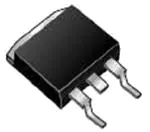
EcoSPARK 300mJ, 400V, N-Channel Current Sensing Ignition IGBT
General Description
Applications
The FGB3040CS is an lgnition IGBT that offers outstanding SCIS capability along with a ratiometric emitter current
sensing capability. This sensing is based on a emitter
active area ratio of 200:1. The output is provided through a
fourth (sense) lead. This signal provides a current level
that is proportional to the main collector to emitter current.
The effective ratio as measured on the sense lead is a
function of the sense output, the collector current and the
gate to emitter drive voltage.
Smart Automotive lgnition Coil Driver Circuits
ECU Based Systems
Distributorless Based Systems
Coil on Plug Based Systems
Features
SCIS Energy = 300mJ at TJ = 25oC
Logic Level Gate Drive
Qualified to AEC Q101
RoHS Compliant
Package
Symbol
Device Maximum Ratings TA = 25°C unless otherwise noted
Symbol
Parameter
BVCER Collector to Emitter Breakdown Voltage (IC = 2mA)
Ratings
430
Units
V
BVECS
Emitter to Collector Breakdown Voltage (IC = 1mA) (Reverse Battery Condition)
24
V
ESCIS25
Self Clamping Inductive Switching Energy (at starting TJ = 25°C)
300
mJ
mJ
ESCIS150 Self Clamping Inductive Switching Energy (at starting TJ = 150°C)
170
IC25
Continuous Collector Current, at VGE = 4.0V, TC = 25°C
21
A
IC110
Continuous Collector Current, at VGE = 4.0V, TC = 110°C
19
A
VGEM
Maximum Continuous Gate to Emitter Voltage
±10
V
Power Dissipation, at TC = 25°C
150
W
1
W/oC
PD
Power Dissipation Derating, for TC > 25oC
TJ
Operating Junction Temperature Range
-40 to 175
o
TSTG
Storage Junction Temperature Range
-40 to 175
oC
TL
Max. Lead Temp. for Soldering (at 1.6mm from case for 10sec)
300
oC
TPKG
Max. Package Temp. for Soldering (Package Body for 10 sec)
260
oC
ESD
Electrostatic Discharge Voltage, HBM model (100pfd, 1500 ohms)
4
kV
@2012 Semiconductor Components Industries, LLC.
October-2017,Rev.3
C
Publication Order Number:
FGB3040CS/D
FGB3040CS 300mJ, 400V, N-Channel Current Sensing Ignition IGBT
FGB3040CS
�Device Marking
3040CS
Device
FGB3040CS
Package
TO-263 6 Lead
Reel Size
300mm
Tape Width
24mm
Quantity
800
3040CS
FGB3040CS
TO-263 6 Lead
Tube
N/A
50
Electrical Characteristics TA = 25°C unless otherwise noted
Symbol
Parameter
Test Conditions
Min
Typ
Max Units
Off State Characteristics
BVCER
ICE = 2mA, VGE = 0,
Collector to Emitter Breakdown Voltage RGE = 1KΩ, See Fig. 17
TJ = -40 to 150oC
370
410
430
V
BVCES
ICE = 10mA, VGE = 0V
Collector to Emitter Breakdown Voltage RGE = 0, See Fig. 17
TJ = -40 to 150oC
390
430
450
V
BVECS
Emitter to Collector Breakdown Voltage
ICE = -75mA, VGE = 0V,
TC = 25°C
30
-
-
V
BVGES
Gate to Emitter Breakdown Voltage
IGES = ±2mA
±12
±14
-
V
IGEO
Gate to Emitter Leakage Current
VGE = ±10V
-
-
±9
μA
ICES
Collector to Emitter Leakage Current
VCES = 250V,
See Fig. 13
-
-
25
μA
TC = 150oC
-
-
1
mA
IECS
Emitter to Collector Leakage Current
VEC = 24V,
See Fig. 13
-
-
1
TC = 150oC
-
-
40
R1
Series Gate Resistance
-
100
-
Ω
TC = 25oC
TC = 25oC
mA
On State Characteristics
VCE(SAT) Collector to Emitter Saturation Voltage ICE = 6A, VGE = 4V
TC = 25oC
See Fig. 5
-
1.3
1.6
V
VCE(SAT) Collector to Emitter Saturation Voltage ICE = 10A, VGE = 4.5V
TC = 150oC
See Fig. 6
-
1.6
1.85
V
-
1.8
2.35
V
VCE = 5V, VGE = 5V
-
37
-
A
-
15
-
nC
1.3
1.6
2.2
0.75
1.1
1.8
VCE(SAT) Collector to Emitter Saturation Voltage ICE = 15A, VGE = 4.5V
ICE(ON)
Collector to Emitter On State Current
o
TC = 150 C
Dynamic Characteristics
QG(ON)
Gate Charge
ICE = 10A, VCE = 12V,
VGE = 5V, See Fig. 16
VGE(TH)
Gate to Emitter Threshold Voltage
ICE = 1mA, VCE = VGE
See Fig. 12
VGEP
Gate to Emitter Plateau Voltage
ICE = 10A, VCE = 12V
-
3.0
-
V
βAREA
Emitter Sense Area Ratio
Sense Area/Total Area
-
1/200
-
-
β5Ω
Emitter Current Sense Ratio
ICE = 8.0A, VGE = 5V, RSENSE = 5 Ω
-
230
-
-
β20Ω
Emitter Current Sense Ratio
ICE = 9.0A, VGE = 5V, RSENSE = 20 Ω
550
640
765
-
-
0.6
4
μs
-
1.5
7
μs
-
4.7
15
μs
-
2.6
15
μs
TJ = 25°C, L = 3.0mHy, ICE = 14.2A,
RG = 1k Ω, VGE = 5V, See Fig. 3&4
-
-
300
mJ
All Packages
-
-
1.0
oC/W
TC = 25oC
TC = 150oC
V
Switching Characteristics
td(ON)R
trR
Current Turn-On Delay Time-Resistive VCE = 14V, RL = 1Ω
VGE = 5V, RG = 1KΩ
Current Rise Time-Resistive
TJ = 25°C, See Fig. 14
td(OFF)L Current Turn-Off Delay Time-Inductive VCE = 300V, L = 500μHy,
VGE = 5V, RG = 1KΩ
Current Fall Time-Inductive
tfL
TJ = 25°C, See Fig. 14
SCIS
Self Clamped inductive Switching
Thermal Characteristics
RθJC
Thermal Resistance Junction to Case
www.onsemi.com
2
FGB3040CS 300mJ, 400V, N-Channel Current Sensing Ignition IGBT
Package Marking and Ordering Information
�0.5
VSENSE, EMITTER SENSE VOLTAGE (mV)
400
ICE = 18A
o
VGE = 5V, TJ = 25 C
ICE = 15A
ICE = 10A
0.3
ICE = 5A
ICE = 3A
ICE = 1A
200
ICE = 0.5A
0.2
100
0.1
0.0
1
10
100
1000
RSENSE, Emitter Sense Resistance (ohms)
35
RG = 1KΩ, VGE = 5V, VCE = 14V
30
25
o
TJ = 25 C
20
15
o
10
TJ = 150 C
5
0
SCIS Curves valid for Vclamp Voltages of
