ON Semiconductor
Is Now
To learn more about onsemi™, please visit our website at
www.onsemi.com
onsemi and and other names, marks, and brands are registered and/or common law trademarks of Semiconductor Components Industries, LLC dba “onsemi” or its affiliates and/or
subsidiaries in the United States and/or other countries. onsemi owns the rights to a number of patents, trademarks, copyrights, trade secrets, and other intellectual property. A listing of onsemi
product/patent coverage may be accessed at www.onsemi.com/site/pdf/Patent-Marking.pdf. onsemi reserves the right to make changes at any time to any products or information herein, without
notice. The information herein is provided “as-is” and onsemi makes no warranty, representation or guarantee regarding the accuracy of the information, product features, availability, functionality,
or suitability of its products for any particular purpose, nor does onsemi assume any liability arising out of the application or use of any product or circuit, and specifically disclaims any and all
liability, including without limitation special, consequential or incidental damages. Buyer is responsible for its products and applications using onsemi products, including compliance with all laws,
regulations and safety requirements or standards, regardless of any support or applications information provided by onsemi. “Typical” parameters which may be provided in onsemi data sheets and/
or specifications can and do vary in different applications and actual performance may vary over time. All operating parameters, including “Typicals” must be validated for each customer application
by customer’s technical experts. onsemi does not convey any license under any of its intellectual property rights nor the rights of others. onsemi products are not designed, intended, or authorized
for use as a critical component in life support systems or any FDA Class 3 medical devices or medical devices with a same or similar classification in a foreign jurisdiction or any devices intended for
implantation in the human body. Should Buyer purchase or use onsemi products for any such unintended or unauthorized application, Buyer shall indemnify and hold onsemi and its officers, employees,
subsidiaries, affiliates, and distributors harmless against all claims, costs, damages, and expenses, and reasonable attorney fees arising out of, directly or indirectly, any claim of personal injury or death
associated with such unintended or unauthorized use, even if such claim alleges that onsemi was negligent regarding the design or manufacture of the part. onsemi is an Equal Opportunity/Affirmative
Action Employer. This literature is subject to all applicable copyright laws and is not for resale in any manner. Other names and brands may be claimed as the property of others.
�FGHL40S65UQ
Product Preview
Field Stop Trench IGBT
40 A, 650 V
Using the novel field stop generation IGBT technology,
ON Semiconductor’s new series of field stop 4th generation of RC
IGBTs offer superior conduction and switching performance and easy
parallel operation. This device is well suited for the resonant or soft
switching application such as induction heating and microwave oven.
www.onsemi.com
40 A, 650 V
VCE(sat) = 1.36 V (Typ.)
Features
•
•
•
•
•
•
•
•
•
•
Maximum Junction Temperature: TJ = 175°C
Positive Temperature Co−efficient for Easy Parallel Operating
High Current Capability
Low Saturation Voltage: VCE(sat) = 1.36 V (Typ.) @IC = 40 A
100% of the Parts tested for ILM (Note 1)
High Input Impedance
Fast Switching
Tighten Parameter Distribution
RoHS Compliant
IGBT with Monolithic Reverse Conducting Diode
C
G
E
G
Typical Applications
C
• Induction Heating
• Microwave Oven
• Soft Switching Application
E
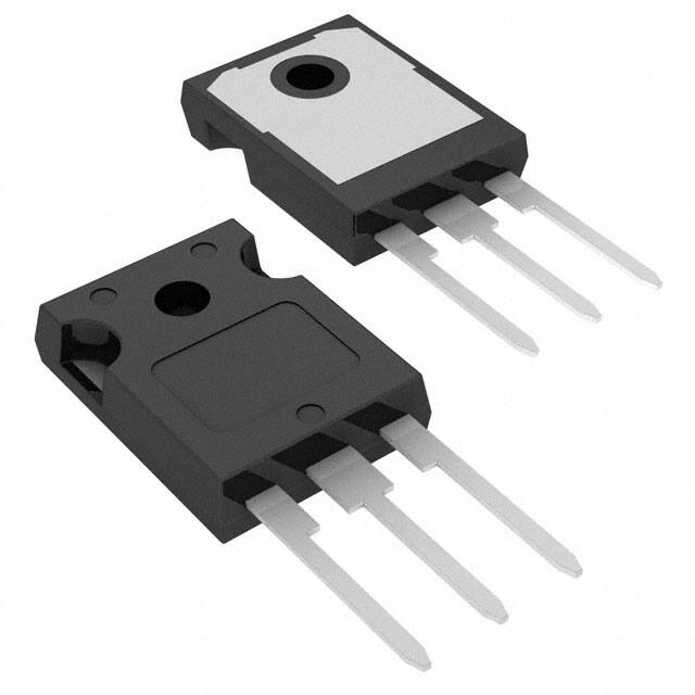
TO−247−3L
CASE 340CX
MARKING DIAGRAM
MAXIMUM RATINGS
Rating
Symbol
Value
Unit
Collector to Emitter Voltage
VCES
650
V
Gate to Emitter Voltage
Transient Gate to Emitter Voltage
VGES
±20
±30
V
IC
80
40
A
Pulsed Collector Current (Note 1)
ILM
120
A
Pulsed Collector Current (Note 2)
ICM
120
A
IF
40
20
A
Pulsed Diode Maximum Forward Current
IFM
120
A
Maximum Power Dissipation
@TC = 25°C
@TC = 100°C
PD
231
115
W
Operating Junction
/ Storage Temperature Range
TJ, TSTG
−55 to
+175
°C
TL
260
°C
Collector Current
@TC = 25°C
@TC = 100°C
Diode Forward Current
@TC = 25°C
@TC = 100°C
Maximum Lead Temp. for Soldering
Purposes, 1/8” from case for 5 seconds
Stresses exceeding those listed in the Maximum Ratings table may damage the
device. If any of these limits are exceeded, device functionality should not be
assumed, damage may occur and reliability may be affected.
1. VCC = 400 V, VGE = 15 V, IC = 120 A, RG = 7 W, Inductive Load, 100% Tested.
2. Repetitive rating: pulse width limited by max. Junction temperature.
© Semiconductor Components Industries, LLC, 2018
May, 2019 − Rev. P0
1
&Y&Z&3&K
FGHL40S65
UQ
&Y
&Z
&3
&K
FGHL40S65UQ
= ON Semiconductor Logo
= Assembly Plant Code
= 3−Digit Data Code
= 2−Digit Lot Traceability Code
= Specific Device Code
ORDERING INFORMATION
Device
Package
Shipping
FGHL40S65UQ
TO−247−3L
30 Units / Rail
This document contains information on a product under
development. ON Semiconductor reserves the right to
change or discontinue this product without notice.
Publication Order Number:
FGHL40S65UQ/D
�FGHL40S65UQ
THERMAL CHARACTERISTICS
Symbol
Value
Unit
Thermal resistance junction−to−case, for IGBT
Rating
RqJC
0.65
°C/W
Thermal resistance junction−to−case, for Diode
RqJC
1.69
°C/W
Thermal resistance junction−to−ambient
RqJA
40
°C/W
ELECTRICAL CHARACTERISTICS (TJ = 25°C unless otherwise specified)
Test Conditions
Parameter
Symbol
Min
Typ
Max
Unit
OFF CHARACTERISTIC
Collector−emitter breakdown voltage,
gate−emitter short−circuited
VGE = 0 V, IC = 1 mA
BVCES
650
−
−
V
Temperature Coefficient of Breakdown Voltage
VGE = 0 V, IC = 1 mA
DBVCES/
DTJ
−
0.5
−
V/°C
Collector−emitter cut−off current, gate−emitter
short−circuited
VGE = 0 V, VCE = 650 V
ICES
−
−
250
mA
Gate leakage current, collector−emitter
short−circuited
VGE = 20 V, VCE = 0 V
IGES
−
−
±400
nA
Gate−emitter threshold voltage
VGE = VCE, IC = 40 mA
VGE(th)
2.5
4.7
6.5
V
Collector−emitter saturation voltage
VGE = 15 V, IC = 40 A
VGE = 15 V, IC = 40 A, TJ = 175°C
VCE(sat)
−
−
1.36
1.6
1.7
−
V
VCE = 30 V, VGE = 0 V, f = 1 MHz
Cies
−
6054
−
pF
Coes
−
36
−
Cres
−
30
−
Qg
−
306
−
Qge
−
30
−
Qgc
−
99
−
td(on)
−
32
−
ON CHARACTERISTIC
DYNAMIC CHARACTERISTIC
Input capacitance
Output capacitance
Reverse transfer capacitance
Gate charge total
Gate to emitter charge
VCE = 400 V, IC = 40 A,
VGE = 15 V
Gate to collector charge
nC
SWITCHING CHARACTERISTIC, INDUCTIVE LOAD
Turn−on delay time
Rise time
TJ = 25°C
VCC = 400 V, IC = 40 A,
RG = 6 W
VGE = 15 V
Inductive Load
tr
−
20
−
td(off)
−
260
−
tf
−
13
−
Turn−on switching loss
EON
−
1760
−
Turn−off switching loss
EOFF
−
362
−
Total switching loss
ETS
−
2122
−
td(on)
−
30
−
tr
−
28
−
td(off)
−
284
−
tf
−
56
−
Turn−on switching loss
EON
−
2050
−
Turn−off switching loss
EOFF
−
590
−
Total switching loss
ETS
−
2640
−
Turn−off delay time
Fall time
Turn−on delay time
Rise time
Turn−off delay time
TJ = 175°C
VCC = 400 V, IC = 40 A,
RG = 6 W
VGE = 15 V
Inductive Load
Fall time
www.onsemi.com
2
ns
mJ
ns
mJ
�FGHL40S65UQ
ELECTRICAL CHARACTERISTICS (TJ = 25°C unless otherwise specified) (continued)
Parameter
Test Conditions
Symbol
Min
Typ
Max
Unit
VF
−
−
1.24
1.24
1.6
−
V
DIODE CHARACTERISTIC
Forward voltage
IF = 20 A
IF = 20 A, TJ = 175°C
Reverse Recovery Energy
IF = 20 A, DlF/Dt = 200 A/ms
EREC
−
359
−
mJ
Diode Reverse Recovery Time
IF = 20 A, DlF/Dt = 200 A/ms
IF = 20 A, DlF/Dt = 200 A/ms,
TJ = 175°C
TRR
−
319
430
−
nS
Diode Reverse Recovery Charge
IF = 20 A, DlF/Dt = 200 A/ms
IF = 20 A, DlF/Dt = 200 A/ms,
TJ = 175°C
QRR
−
1853
3007
−
nC
www.onsemi.com
3
�FGHL40S65UQ
TYPICAL CHARACTERISTICS
120
20 V
TJ = 25°C
15 V
12 V
Collector Current, IC [A]
Collector Current, IC [A]
120
10 V
80
VGE = 8 V
40
0
0
1
80
3
2
3
Figure 1. Typical Output Characteristics
Figure 2. Typical Output Characteristics
3
Common Emitter
VGE = 15 V
TJ = 25°C
TJ = 175°C
80
40
0
1
Common Emitter
VGE = 15 V
2.5
2
40 A
1.5
IC = 20 A
0
2
80 A
3
−100
Collector−Emitter Voltage, VCE [V]
−50
0
50
20
Collector−Emitter Voltage, VCE [V]
Common Emitter
TJ = 25°C
12
8
40 A
4
150
200
Figure 4. Saturation Voltage vs. Case Temperature
at Variant Current Level
20
16
100
Collector−Emitter Case Temperature, TC [°C]
Figure 3. Typical Saturation Voltage Characteristics
Collector−Emitter Voltage, VCE [V]
1
Collector−Emitter Voltage, VCE [V]
Collector−Emitter Voltage, VCE [V]
Collector Current, IC [A]
0
Collector−Emitter Voltage, VCE [V]
120
0
VGE = 8 V
40
0
2
20 V
15 V
12 V
10 V
TJ = 175°C
80 A
IC = 20 A
0
Common Emitter
TJ = 175°C
16
12
8
IC = 20 A
4
40 A
80 A
0
0
4
8
12
16
20
0
Gate−Emitter Voltage, VGE [V]
4
8
12
16
Gate−Emitter Voltage, VGE [V]
Figure 6. Saturation Voltage vs VGE
Figure 5. Saturation Voltage vs VGE
www.onsemi.com
4
20
�FGHL40S65UQ
TYPICAL CHARACTERISTICS (continued)
15
Gate−Emitter Voltage, VGE[V]
Capacitance [pF]
VCC = 200 V
Cies
10000
1000
Coes
100
Cres
Common Emitter
VGE = 0 V, f = 1 MHz
TJ = 25°C
10
Common Emitter
TJ = 25°C
12
300 V
400 V
9
6
3
0
1
1
10
30
0
80
160
240
320
Collector−Emitter Voltage, VCE [V]
Gate Charge, QG [nC]
Figure 7. Capacitance Characteristics
Figure 8. Gate Charge Characteristics
10000
100
td(off)
Switching Time [ns]
tr
Switching Time [ns]
400
td(on)
10
Common Emitter
VCC = 400 V,
VGE = 15 V, Ic = 40 A
TJ = 25°C
TJ = 175°C
1000
tf
100
Common Emitter
VCC = 400 V,
VGE = 15 V, Ic = 40 A
TJ = 25°C
TJ = 175°C
10
1
1
0
10
20
30
40
0
50
10
20
30
40
50
Gate Resistance, RG [ W]
Gate Resistance, RG [W]
Figure 9. Turn−on Characteristics vs. Gate Resistance
Figure 10. Turn−Off Characteristics vs. Gate
Resistance
1000
5000
EOFF
Switching Time [ns]
Switching Loss [mJ]
EON
1000
Common Emitter
VCC = 400 V,
VGE =
15V,
V,RICG == 40
=15
6 WA
TJC == 25°C
25°C
TJC == 175°C
175°C
100
tr
100
td(on)
Common Emitter
VCC = 400 V,
VGE = 15 V, RG = 6 W
TJ = 25°C
TJ = 175°C
10
1
5
15
25
40
0
50
30
60
90
120
150
Gate Resistance, RG [W]
Collector Current, IC [A]
Figure 11. Switching Loss vs Gate Resistance
Figure 12. Turn−On Characteristics vs. Collector
Current
www.onsemi.com
5
�FGHL40S65UQ
TYPICAL CHARACTERISTICS (continued)
10000
1000
EON
100
Common Emitter
Vcc = 400 V
VGE = 15 V, RG = 6 W
TJ = 25°C
TJ = 175°C
10
1
0
30
60
Common Emitter
Vcc = 400 V
VGE = 15 V, RG = 6 W
TJ = 25°C
TJ = 175°C
100
10
120
0
60
90
120
150
Figure 13. Turn−Off Characteristics vs.
Collector Current
Figure 14. Switching Loss vs. Collector Current
300
Square Wave
TJ ≤ 175°C, D = 0.5,
VCE = 400 V,
VGE = 15/0 V, RG = 6 W
TJ = 25°C
200
100
TJ = 75°C
150
TJ = 100°C
100
10 ms
DC
1 ms
10 ms
1
*Notes:
1. TJ = 25°C
2. TJ = 175°C
3. Single Pulse
0.1
0
1000
10000
100000
1
1000000
100
1000
Collector−Emitter Voltage, VCE [V]
Figure 15. Load Current vs Frequency
Figure 16. SOA Characteristics (FBSOA)
16
TJ = 175°C
TJ = 75°C
10
0
10
Switching Frequency, f [Hz]
TJ = 25°C
100
100 ms
10
50
1
30
Collector Current, IC [A]
Collector Current, IC [A]
Collector Current, IC [A]
90
EOFF
1000
Collector Current, IC [A]
250
Forward Current, IF [A]
Switching Loss [mJ]
tf
Reverse Recovery Current, IRR [A]
Switching Time [ns]
td(off)
1
2
3
4
14
di/dt = 200 A/ms
12
10
6
4
TJ = 25°C
TJ = 175°C
2
0
5
di/dt = 100 A/ms
8
0
10
20
30
Forward Voltage, VF [V]
Forward Current, IF [A]
Figure 17. Forward Characteristics
Figure 18. Reverse Recovery Current
www.onsemi.com
6
40
�FGHL40S65UQ
TYPICAL CHARACTERISTICS (continued)
4000
600
Stored Recovery Charge , QRR [nC]
di/dt = 200 A/ms
500
400
300
di/dt = 100 A/ms
200
100
0
10
20
30
3500
3000
di/dt = 200 A/ms
2500
di/dt = 100 A/ms
2000
1500
1000
TJ = 25°C
TJ = 175°C
500
0
40
0
10
Forward Current, IF [A]
20
Figure 20. Stored Charge
1
0.5
0.1
0.2
0.1
PDM
t1
t2
0.05
0.02
0.01
Single Pulse
0.01
10−5
10−4
Duty Factor, D = t1/t2
Paek TJ = Pdm × Zthjc + TC
10−3
10−2
10−1
100
101
Rectangular Pulse Duration [sec]
Figure 21. Transient Thermal Impedance of IGBT
5
1
0.5
0.2
0.1
0.1
0.05
0.02
0.01
PDM
t1
t2
Duty Factor, D = t1/t2
Paek TJ = Pdm × Zthjc + TC
Single Pulse
0.01
10−5
10−4
30
Forward Current, IF [A]
Figure 19. Reverse Recovery Time
Thermal Response [Zthjc]
0
TJ = 25°C
TJ = 175°C
Thermal Response [Zthjc]
Reverse Recovery Time, tRR [ns]
700
10−3
10−2
10−1
100
Rectangular Pulse Duration [sec]
Figure 22. Transient Thermal Impedance of Diode
www.onsemi.com
7
101
40
�FGHL40S65UQ
TO−247−3LD
CASE 340CX
ISSUE O
www.onsemi.com
8
�FGHL40S65UQ
ON Semiconductor and
are trademarks of Semiconductor Components Industries, LLC dba ON Semiconductor or its subsidiaries in the United States and/or other countries.
ON Semiconductor owns the rights to a number of patents, trademarks, copyrights, trade secrets, and other intellectual property. A listing of ON Semiconductor’s product/patent
coverage may be accessed at www.onsemi.com/site/pdf/Patent−Marking.pdf. ON Semiconductor reserves the right to make changes without further notice to any products herein.
ON Semiconductor makes no warranty, representation or guarantee regarding the suitability of its products for any particular purpose, nor does ON Semiconductor assume any liability
arising out of the application or use of any product or circuit, and specifically disclaims any and all liability, including without limitation special, consequential or incidental damages.
Buyer is responsible for its products and applications using ON Semiconductor products, including compliance with all laws, regulations and safety requirements or standards,
regardless of any support or applications information provided by ON Semiconductor. “Typical” parameters which may be provided in ON Semiconductor data sheets and/or
specifications can and do vary in different applications and actual performance may vary over time. All operating parameters, including “Typicals” must be validated for each customer
application by customer’s technical experts. ON Semiconductor does not convey any license under its patent rights nor the rights of others. ON Semiconductor products are not
designed, intended, or authorized for use as a critical component in life support systems or any FDA Class 3 medical devices or medical devices with a same or similar classification
in a foreign jurisdiction or any devices intended for implantation in the human body. Should Buyer purchase or use ON Semiconductor products for any such unintended or unauthorized
application, Buyer shall indemnify and hold ON Semiconductor and its officers, employees, subsidiaries, affiliates, and distributors harmless against all claims, costs, damages, and
expenses, and reasonable attorney fees arising out of, directly or indirectly, any claim of personal injury or death associated with such unintended or unauthorized use, even if such
claim alleges that ON Semiconductor was negligent regarding the design or manufacture of the part. ON Semiconductor is an Equal Opportunity/Affirmative Action Employer. This
literature is subject to all applicable copyright laws and is not for resale in any manner.
PUBLICATION ORDERING INFORMATION
LITERATURE FULFILLMENT:
Literature Distribution Center for ON Semiconductor
19521 E. 32nd Pkwy, Aurora, Colorado 80011 USA
Phone: 303−675−2175 or 800−344−3860 Toll Free USA/Canada
Fax: 303−675−2176 or 800−344−3867 Toll Free USA/Canada
Email: orderlit@onsemi.com
◊
N. American Technical Support: 800−282−9855 Toll Free
USA/Canada
Europe, Middle East and Africa Technical Support:
Phone: 421 33 790 2910
www.onsemi.com
9
ON Semiconductor Website: www.onsemi.com
Order Literature: http://www.onsemi.com/orderlit
For additional information, please contact your local
Sales Representative
FGHL40S65UQ/D
�