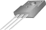
FGPF70N30T
300V, 70A PDP IGBT
tm
Features
General Description
• High current capability
Using Novel Trench IGBT Technology, Fairchild’s new sesries
of trench IGBTs offer the optimum performance for PDP applications where low conduction and switching losses are essential.
• Low saturation voltage: VCE(sat) =1.5V @ IC = 40A
• High input impedance
• Fast switching
• RoHS complaint
Application
. PDP System
GC E
TO-220F
Absolute Maximum Ratings
Symbol
Description
Ratings
Units
300
V
VCES
Collector-Emitter Voltage
VGES
Gate-Emitter Voltage
±30
V
IC pulse(1)*
Pulsed Collector Current
@ TC = 25oC
160
A
Maximum Power Dissipation
@ TC = 25oC
49.2
W
PD
Maximum Power Dissipation
o
@ TC = 100 C
19.7
W
TJ
Operating Junction Temperature
-55 to +150
oC
Tstg
Storage Temperature Range
-55 to +150
o
C
TL
Maximum Lead Temp. for soldering
Purposes, 1/8” from case for 5 seconds
300
o
C
Thermal Characteristics
Symbol
RθJC(IGBT)
RθJA
Parameter
Thermal Resistance, Junction-to-Case
Thermal Resistance, Junction-to-Ambient
Typ.
Max.
--
2.54
o
C/W
62.5
o
C/W
--
Units
Notes:
(1)Repetitive test , pluse width = 100usec , Duty = 0.1
* Ic_pluse limited by max Tj
©2007 Fairchild Semiconductor Corporation
FGPF70N30T Rev. A
1
www.fairchildsemi.com
FGPF70N30T 300V, 70A PDP Trench IGBT
June 2007
�Device Marking
Device
Package
Packaging
Type
Qty per Tube
Max Qty
per Box
FGPF70N30T
FGPF70N30TTU
TO-220F
Tube
50ea
-
Electrical Characteristics T
C
Symbol
= 25oC unless otherwise noted
Parameter
Test Conditions
Min.
Typ.
Max.
Units
Off Characteristics
BVCES
Collector-Emitter Breakdown Voltage
VGE = 0V, IC = 250uA
300
--
--
V
∆BVCES/
∆TJ
Temperature Coefficient of Breakdown
Voltage
VGE = 0V, IC = 250uA
--
0.2
--
V/oC
ICES
Collector Cut-Off Current
VCE = VCES, VGE = 0V
--
--
250
uA
IGES
G-E Leakage Current
VGE = VGES, VCE = 0V
--
--
± 400
nA
IC = 250uA, VCE = VGE
3.0
4.5
5.5
V
IC =20A, VGE = 15V
--
1.2
1.5
V
IC =40A, VGE = 15V
--
1.5
--
V
IC =70A, VGE = 15V
TC = 25oC
--
1.8
--
V
IC = 70A, VGE = 15V
TC = 125oC
--
1.9
--
V
--
3000
--
pF
VCE = 30V, VGE = 0V
f = 1MHz
--
160
--
pF
--
110
--
pF
On Characteristics
VGE(th)
VCE(sat)
G-E Threshold Voltage
Collector to Emitter
Saturation Voltage
Dynamic Characteristics
Cies
Input Capacitance
Coes
Output Capacitance
Cres
Reverse Transfer Capacitance
Switching Characteristics
td(on)
Turn-On Delay Time
tr
Rise Time
td(off)
Turn-Off Delay Time
tf
Fall Time
td(on)
Turn-On Delay Time
tr
Rise Time
td(off)
Turn-Off Delay Time
tf
Fall Time
Qg
Total Gate Charge
Qge
Gate-Emitter Charge
Qgc
Gate-Collector Charge
VCC = 200V, IC = 40A
RG = 15Ω, VGE = 15V
Resistive Load, TC = 25oC
VCC = 200V, IC = 40A
RG = 15Ω, VGE = 15V
Resistive Load, TC = 125oC
VCE = 200V, IC = 40A
VGE = 15V
2
FGPF70N30T Rev. A
--
32
--
ns
--
90
--
ns
--
175
--
ns
--
170
300
ns
--
30
--
ns
--
90
--
ns
--
185
--
ns
--
235
--
ns
--
125
--
nC
--
25
--
nC
--
55
--
nC
www.fairchildsemi.com
FGPF70N30T 300V, 70A PDP Trench IGBT
Package Marking and Ordering Information
�Figure 1. Typical Output Characteristics
160
160
o
TC = 25 C
20V
15V
12V
120
80
VGE = 8V
40
2
4
6
Collector-Emitter Voltage, VCE [V]
80
VGE = 8V
40
0
8
Figure 3. Typical Saturation Voltage
Characteristics
2
4
6
Collector-Emitter Voltage, VCE [V]
8
Figure 4. Transfer Characteristics
160
160
Common Emitter
Common Emitter
VGE = 15V
100 VCE = 20V
o
o
TC = 25 C
120
Collector Current, IC [A]
Collector Current, IC [A]
20V
15V
12V
0
0
o
TC = 125 C
80
40
0
0
1
2
3
Collector-Emitter Voltage, VCE [V]
Collector-Emitter Voltage, VCE [V]
40A
IC = 20A
12
3
Common Emitter
o
T = 25 C
C
16
12
8
40A
4
70A
0
50
75
100
125
o
Collector-EmitterCase Temperature, TC [ C]
FGPF70N30T Rev. A
4
6
8
10
Gate-Emitter Voltage,VGE [V]
20
1.6
0.8
25
10
Figure 6. Saturation Voltage vs. VGE
70A
1.2
o
TC = 125 C
2
Common Emitter
VGE = 15V
2.0
TC = 25 C
1
4
Figure 5. Saturation Voltage vs. Case
Temperature at Variant Current Level
2.4
10V
120
0
Collector-Emitter Voltage, VCE [V]
o
TC = 125 C
10V
Collector Current, IC [A]
Collector Current, IC [A]
Figure 2. Typical Output Characteristics
IC = 20A
4
8
12
16
Gate-Emitter Voltage, VGE [V]
20
www.fairchildsemi.com
FGPF70N30T 300V, 70A PDP Trench IGBT
Typical Performance Characteristics
�Figure 7. Saturation Voltage vs. VGE
6000
20
Collector-Emitter Voltage, VCE [V]
Figure 8. Capacitance Characteristics
Common Emitter
VGE = 0V, f = 1MHz
Common Emitter
o
T = 125 C
5000
C
o
TC = 25 C
Capacitance [pF]
16
12
8
Ciss
3000
2000
Coss
40A
4
1000
70A
0
4000
IC = 20A
4
Crss
0
8
12
16
Gate-Emitter Voltage, VGE [V]
1
20
Figure 9. Gate Charge Characteristics
30
10
Collector-Emitter Voltage, VCE [V]
Figure 10. SOA Characteristics
15
Common Emitter
IC MAX (Pulsed)
12
Collector Current, IC [A]
Gate-Emitter Voltage, VGE [V]
o
TC = 25 C
Vcc = 200V
100V
9
6
100µs
100
1ms
10
IC MAX (Continuous)
1
Single Nonrepetitive
o
Pulse TC = 25 C
Curves must be derated
linearly with increase
in temperature
0.1
3
0.01
0.1
0
0
30
60
90
120
Gate Charge, Qg [nC]
150
10ms
DC Operation
1
10
100
Collector - Emitter Voltage, VCE [V]
500
Figure 12. Turn-off Characteristics vs.
Gate Resistance
Figure 11. Turn-on Characteristics vs.
Gate Resistance
3000
300
Switching Time [ns]
Switching Time [ns]
1000
100
tr
Common Emitter
VCC = 200V, VGE = 15V
IC = 40A
td(on)
tf
100
Common Emitter
VCC = 200V, VGE = 15V
IC = 40A
td(off)
o
o
TC = 25 C
TC = 25 C
o
o
TC = 125 C
TC = 125 C
10
10
0
20
40
60
80
0
100
Gate Resistance, RG [Ω]
40
60
80
100
Gate Resistance, RG [Ω ]
4
FGPF70N30T Rev. A
20
www.fairchildsemi.com
FGPF70N30T 300V, 70A PDP Trench IGBT
Typical Performance Characteristics (Continued)
�Figure 13. Turn-on Characteristics vs.
Collector Current
500
Figure 14. Turn-off Characteristics vs.
Collector Current
1000
Common Emitter
VGE = 15V, RG = 15Ω
Common Emitter
VGE = 15V, RG = 15Ω
o
o
TC = 25 C
TC = 25 C
tr
TC = 125 C
o
100
td(on)
10
0
20
40
60
80
TC = 125 C
Switching Time [ns]
Switching Time [ns]
o
tf
td(off)
tf
100
100
0
20
Collector Current, IC [A]
40
60
80
100
Collector Current, IC [A]
Figure 15. Switching Loss vs. Gate Resistance
Figure 16. Switching Loss vs. Collector Current
10000
2000
Common Emitter
VGE = 15V, RG = 15Ω
1000
o
Eoff
TC = 25 C
100
Switching Loss [uJ]
Switching Loss [uJ]
o
Eon
Common Emitter
VCC = 200V, VGE = 15V
IC = 40A
TC = 125 C
1000
100
Eon
o
TC = 25 C
Eoff
o
TC = 125 C
10
0
20
40
60
80
Gate Resistance, RG [Ω]
10
100
0
20
40
60
80
100
Collector Current, IC [A]
Figure 17. Transient Thermal Impedance of IGBT
Thermal Response [Zthjc]
10
0.5
1
0.2
0.1
0.05
PDM
0.1 0.02
t1
t2
Duty Factor, D = t1/t2
Peak Tj = Pdm x Zthjc + TC
0.01
single pulse
0.01
1E-4
1E-3
0.01
0.1
1
Rectangular Pulse Duration [sec]
5
FGPF70N30T Rev. A
10
100
www.fairchildsemi.com
FGPF70N30T 300V, 70A PDP Trench IGBT
Typical Performance Characteristics (Continued)
�3.30 ±0.10
10.16 ±0.20
2.54 ±0.20
ø3.18 ±0.10
(7.00)
(1.00x45°)
15.87 ±0.20
15.80 ±0.20
6.68 ±0.20
(0.70)
0.80 ±0.10
0°
(3
9.75 ±0.30
MAX1.47
)
#1
+0.10
0.50 –0.05
2.54TYP
[2.54 ±0.20]
2.54TYP
[2.54 ±0.20]
9.40 ±0.20
6
FGPF70N30T Rev. A
2.76 ±0.20
4.70 ±0.20
0.35 ±0.10
www.fairchildsemi.com
FGPF70N30T 300V, 70A PDP Trench IGBT
TO-220F
�TRADEMARKS
The following are registered and unregistered trademarks and service marks Fairchild Semiconductor owns or is authorized to use and is not
intended to be an exhaustive list of all such trademarks.
®
ACEx
Build it Now™
CorePLUS™
CROSSVOLT™
CTL™
Current Transfer Logic™
®
EcoSPARK
FACT Quiet Series™
®
FACT
®
FAST
FastvCore™
FPS™
®
FRFET
SM
Global Power Resource
Green FPS™
®
POWEREDGE
Power-SPM™
®
PowerTrench
Programmable Active Droop™
®
QFET
QS™
QT Optoelectronics™
Quiet Series™
RapidConfigure™
SMART START™
®
SPM
STEALTH™
SuperFET™
SuperSOT™-3
SuperSOT™-6
Green FPS™ e-Series™
GTO™
i-Lo™
IntelliMAX™
ISOPLANAR™
MegaBuck™
MICROCOUPLER™
MicroFET™
MicroPak™
Motion-SPM™
®
OPTOLOGIC
®
OPTOPLANAR
PDP-SPM™
®
Power220
®
Power247
SuperSOT™-8
SyncFET™
®
The Power Franchise
™
TinyBoost™
TinyBuck™
®
TinyLogic
TINYOPTO™
TinyPower™
TinyPWM™
TinyWire™
μSerDes™
®
UHC
UniFET™
VCX™
DISCLAIMER
FAIRCHILD SEMICONDUCTOR RESERVES THE RIGHT TO MAKE CHANGES WITHOUT FURTHER NOTICE TO ANY PRODUCTS
HEREIN TO IMPROVE RELIABILITY, FUNCTION, OR DESIGN. FAIRCHILD DOES NOT ASSUME ANY LIABILITY ARISING OUT OF THE
APPLICATION OR USE OF ANY PRODUCT OR CIRCUIT DESCRIBED HEREIN; NEITHER DOES IT CONVEY ANY LICENSE UNDER ITS
PATENT RIGHTS, NOR THE RIGHTS OF OTHERS. THESE SPECIFICATIONS DO NOT EXPAND THE TERMS OF FAIRCHILD’S
WORLDWIDE TERMS AND CONDITIONS, SPECIFICALLY THE WARRANTY THEREIN, WHICH COVERS THESE PRODUCTS.
LIFE SUPPORT POLICY
FAIRCHILD’S PRODUCTS ARE NOT AUTHORIZED FOR USE AS CRITICAL COMPONENTS IN LIFE SUPPORT DEVICES OR
SYSTEMS WITHOUT THE EXPRESS WRITTEN APPROVAL OF FAIRCHILD SEMICONDUCTOR CORPORATION.
As used herein:
1. Life support devices or systems are devices or systems
which, (a) are intended for surgical implant into the body or
(b) support or sustain life, and (c) whose failure to perform
when properly used in accordance with instructions for use
provided in the labeling, can be reasonably expected to
result in a significant injury of the user.
2. A critical component in any component of a life support,
device, or system whose failure to perform can be
reasonably expected to cause the failure of the life support
device or system, or to affect its safety or effectiveness.
PRODUCT STATUS DEFINITIONS
Definition of Terms
Datasheet Identification
Product Status
Advance Information
Formative or In Design
This datasheet contains the design specifications for product
development. Specifications may change in any manner without notice.
Definition
Preliminary
First Production
This datasheet contains preliminary data; supplementary data will be
published at a later date. Fairchild Semiconductor reserves the right to
make changes at any time without notice to improve design.
No Identification Needed
Full Production
This datasheet contains final specifications. Fairchild Semiconductor
reserves the right to make changes at any time without notice to improve
design.
Obsolete
Not In Production
This datasheet contains specifications on a product that has been
discontinued by Fairchild Semiconductor. The datasheet is printed for
reference information only.
Rev. I29
© 2007 Fairchild Semiconductor Corporation
www.fairchildsemi.com
�