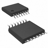
FHP3350, FHP3450
Triple and Quad Voltage Feedback Amplifiers
Features
Description
■ 0.1dB gain flatness to 30MHz
The FHP3350 and FHP3450 are low-cost, high-performance,
voltage-feedback amplifiers designed for video applications.
These triple and quad amplifiers consume only 3.6mA of supply
current per channel and are capable of driving dual (75Ω)
video loads while providing 0.1dB of gain flatness to 30MHz.
Consumer video applications also benefit from the low 0.07%
differential gain and 0.03° differential phase errors. The FHP3350
offers three outputs that can be put into a high-impedance
disable state to allow for video multiplexing or minimize power
consumption.
■ 0.07%/0.03° differential gain/phase error
■ 210MHz full power -3dB bandwidth at G = 2
■ 1,100V/μs slew rate
■ ±55mA output current (drives dual video load)
■ ±83mA output short-circuit current
■ Output swings to within 1.3V of either rail
■ 3.6mA supply current per amplifier
■ Minimum stable gain of 3dB or 1.5V/V
■ FHP3350 - improved replacement for RC6333
These amplifiers are designed to operate from 5V (±2.5V) to 12V
(±6V) supplies. The outputs swing to within 1.3V of either supply
rail to accommodate video signals on a single 5V supply.
■ FHP3450 - improved replacement for RC6334
■ Fully specified at +5V, and ±5V supplies
The FHP3350 and FHP3450 are designed on a complementary
bipolar process. They provide 210MHz of full-power bandwidth
and 1,100V/µs of slew rate at a supply voltage of ±5V. The
combination of high performance, low power, and excellent video
performance make these amplifiers well suited for use in many
digital consumer video appliances as well as many generalpurpose, high-speed applications.
Applications
■ Video driver
■ RGB driver
■ ADC buffer
■ S-video amp
■ Active filters
Typical Application – Driving Dual Video Loads
+Vs
+IN
75Ω
Cable
75Ω
75Ω
75Ω
Cable
75Ω
75Ω
Cable
OUT
75Ω
Rf
Rg
OUT
75Ω
-Vs
Ordering Information
Package
Lead Free
Operating Temp
Range
Packaging
Method
FHP3350IMTC14X
FHP3350IM14X
TSSOP-14
Yes
-40°C to +85°C
Reel
SOIC-14
Yes
-40°C to +85°C
Reel
FHP3450IMTC14X
TSSOP-14
Yes
-40°C to +85°C
Reel
SOIC-14
Yes
-40°C to +85°C
Reel
Part Number
FHP3450IM14X
Moisture sensitivity level for all parts is MSL-1.
FHP3350, FHP3450 Rev. 1.0.3
www.fairchildsemi.com
FHP3350, FHP3450 Triple and Quad Voltage Feedback Amplifiers
December 2006
�NC or DISABLE1
1
14
OUT2
NC or DISABLE2
2
13
-IN2
NC or DISABLE3
3
12
+IN2
+Vs
4
11
-Vs
+IN1
5
10
+IN3
-IN1
6
9
-IN3
OUT1
7
8
OUT3
FHP3350
TSSOP-14
FHP3450 Pin Configurations
OUT1
14
1
OUT4
-IN1
2
13
-IN4
+IN1
3
12
+IN4
11
-Vs
10
+IN3
+Vs
4
+IN2
5
FHP3450
TSSOP-14
-IN2
6
9
-IN3
OUT2
7
8
OUT3
FHP3350, FHP3450 Rev. 1.0.3
FHP3350 Pin Assignments
Pin#
Pin
Description
1
NC or DISABLE1
Channel 1 ENABLED if pin is left open or
pulled above VON, DISABLED if pin is grounded or pulled below VOFF
2
NC or DISABLE2
Channel 2 ENABLED if pin is left open or
pulled above VON, DISABLED if pin is grounded or pulled below VOFF
3
NC or DISABLE3
Channel 3 ENABLED if pin is left open or
pulled above VON, DISABLED if pin is grounded or pulled below VOFF
4
+Vs
Positive supply
5
+IN1
Positive Input, channel 1
6
-IN1
Negative Input, channel 1
7
OUT1
Output, channel 1
8
OUT3
Output, channel 3
9
-IN3
Negative Input, channel 3
10
+IN3
Positive Input, channel 3
11
-Vs
12
+IN2
Negative supply
Positive Input, channel 2
13
-IN2
Negative Input, channel 2
14
OUT2
Output, channel 2
FHP3450 Pin Assignments
Pin#
Pin
1
OUT1
Description
Output, channel 1
2
-IN1
Negative Input, channel 1
3
+IN1
Positive Input, channel 1
4
+Vs
Positive supply
5
+IN2
Positive Input, channel 2
6
-IN2
Negative Input, channel 2
7
OUT2
Output, channel 2
8
OUT3
Output, channel 3
9
-IN3
Negative Input, channel 3
10
+IN3
Positive Input, channel 3
11
-Vs
12
+IN4
Positive Input, channel 4
13
-IN4
Negative Input, channel 4
14
OUT4
�
Negative supply
Output, channel 4
www.fairchildsemi.com
FHP3350, FHP3450 Triple and Quad Voltage Feedback Amplifiers
FHP3350 Pin Configurations
�The “Absolute Maximum Ratings” are those values beyond which the safety of the device cannot be guaranteed. The device should not
be operated at these limits. The parametric values defined in the Electrical Characteristics tables are not guaranteed at the absolute
maximum ratings. The “Recommended Operating Conditions” table defines the conditions for actual device operation.
Parameter
Min.
Max.
Unit
0
12.6
V
-Vs - 0.5V
+Vs +0.5V
V
Supply Voltage
Input Voltage Range
Reliability Information
Parameter
Min.
Typ.
Junction Temperature
Storage Temperature Range
-65
Lead Temperature (Soldering, 10s)
Max.
Unit
150
°C
150
°C
300
°C
14-Lead TSSOP1
160
°C/W
14-Lead SOIC1
148
°C/W
Note:
1. Package thermal resistance (θJA), JDEC standard, multi-layer test boards, still air.
Assumed power is concentrated in one channel, θJA is lower if power is distributed in all channels.
ESD Protection
ESD Protection
FHP3350
Package
FHP3450
SOIC
TSSOP
SOIC
Human Body Model (HBM)
2kV
2kV
2kV
2kV
Charged Device Model (CDM)
2kV
2kV
2kV
1.5kV
250V
250V
TBD
TBD
Min.
Typ.
Max.
Unit
-40
+85
°C
3
12
V
Machine Model (MM)
TSSOP
Recommended Operating Conditions
Parameter
Operating Temperature Range
Supply Voltage Range
FHP3350, FHP3450 Rev. 1.0.3
�
www.fairchildsemi.com
FHP3350, FHP3450 Triple and Quad Voltage Feedback Amplifiers
Absolute Maximum Ratings
�TA = 25°C, VS = 5V, Rf = 249Ω, RL = 150Ω to VS/2, G = 2; unless otherwise noted.
Symbol
Parameter
Conditions
Min.
Typ.
Max.
Units
Frequency Domain Response
BWss
-3dB Bandwidth
No Peaking, G = +2, VOUT = 0.2Vpp
190
MHz
BWLs
Full-Power Bandwidth
No Peaking, G = +2, VOUT = 2Vpp
190
MHz
BW0.1dB
0.1dB Gain Flatness - Large Signal
G = +2, VOUT = 2Vpp
35
MHz
2.0
ns
Time Domain Response
tR, tF
Rise and Fall Time
VOUT = 0.2V step
tS
Settling Time to 0.1%
VOUT = 2V step
20
ns
OS
Overshoot
VOUT = 0.2V step
2.5
%
SR
Slew Rate
2V step. G = -1
800
V/μs
Distortion/Noise Response
HD2
2nd Harmonic Distortion
VOUT = 2Vpp, 5MHz
-70
dBc
HD3
3rd Harmonic Distortion
VOUT = 2Vpp, 5MHz
-80
dBc
THD
Total Harmonic Distortion
VOUT = 2Vpp, 5MHz
-69
dB
DG
Differential Gain
NTSC (3.58MHz); AC coupled
0.08
%
DP
Differenital Phase
NTSC (3.58MHz); AC coupled
0.02
°
en
Input Voltage Noise
> 100kHz
8.5
nV/Hz
in
Input Current Noise
> 100kHz
1
pA/Hz
XTALK
Crosstalk
at 5MHz
-70
dB
1
mV
DC Performance
VIO
dVIO
Ibn
dIbn
Input Offset Voltage
Average Drift
10
μV/°C
Input Bias Current
±50
nA
Average Drift
0.33
nA/°C
±50
nA
IIO
Input Offset Current
PSRR
Power Supply Rejection Ratio
DC
75
dB
AOL
Open Loop Gain
DC
55
dB
IS
Supply Current per Amplifier
ISD
Disable Supply Current per Amp
3.0
mA
Disable Mode
35
μA
5MHz
-60
dB
3
pF
5MHz
-85
dB
Disable Characteristics
OFFISO
Off Isolation
OFFCOUT
Off Output Capacitance
CHISO
Channel-to-Channel Isolation
TON
Turn-On Time
300
ns
TOFF
Turn-Off Time
80
ns
VOFF
Power Down Input Voltage
DISABLE pins; disabled if pin is
grounded or pulled below VOFF
VON
Enable Input Voltage
DISABLE pins; enabled if pin is left
open or pulled above VON
FHP3350, FHP3450 Rev. 1.0.3
�
+Vs - 3.1
+Vs - 1.9
V
V
www.fairchildsemi.com
FHP3350, FHP3450 Triple and Quad Voltage Feedback Amplifiers
Electrical Characteristics at +5V
�TA = 25°C, VS = 5V, Rf = 249Ω, RL = 150Ω to VS/2, G = 2; unless otherwise noted.
Symbol
Parameter
Conditions
Min.
Typ.
Max.
Units
Input Characteristics
RIN
Input Resistance
CIN
Input Capacitance
CMIR
Input Common Mode Voltage Range
CMRR
Common Mode Rejection Ratio
DC, VCM = 1.5V to 3.5V
70
MΩ
1
pF
1.2 to 3.8
V
90
dB
1 to 4
V
1.1 to 3.9
V
Output Characteristics
RL = 2kΩ to Vs/2
VO
Output Voltage Swing
RL = 150Ω to Vs/2
IOUT
Linear Output Current
VO = +Vs/2
±50
mA
ISC
Short-Circuit Output Current
VO = shorted to +Vs or GND
±75
mA
FHP3350, FHP3450 Rev. 1.0.3
�
www.fairchildsemi.com
FHP3350, FHP3450 Triple and Quad Voltage Feedback Amplifiers
Electrical Characteristics at +5V (Continued)
�TA = 25°C, VS = ±5V, Rf = 249Ω, RL = 150Ω to GND, G = 2; unless otherwise noted.
Symbol
Parameter
Conditions
Min.
Typ.
Max.
Units
Frequency Domain Response
BWss
-3dB Bandwidth
No Peaking, G = +2, VOUT = 0.2Vpp
210
MHz
BWLs
Full-Power Bandwidth
No Peaking, G = +2, VOUT = 2Vpp
210
MHz
BW0.1dB
0.1dB Gain Flatness - Large Signal
G = +2, VOUT = 2Vpp
30
MHz
BW0.1dBss
0.1dB Gain Flatness - Small Signal
G = +2, VOUT = 0.2Vpp
50
MHz
Time Domain Response
tR, tF
Rise and Fall Time
VOUT = 0.2V step
2
ns
tS
Settling Time to 0.1%
VOUT = 2V step
20
ns
OS
Overshoot
VOUT = 0.2V step
1
%
SR
Slew Rate
2V step. G = -1
1100
V/μs
-70
dBc
Distortion / Noise Response
HD2
2nd Harmonic Distortion
VOUT = 2Vpp, 5MHz
HD3
3rd Harmonic Distortion
VOUT = 2Vpp, 5MHz
-74
dBc
THD
Total Harmonic Distortion
VOUT = 2Vpp, 5MHz
-68
dB
DG
Differential Gain
NTSC (3.58MHz); AC coupled
0.07
%
DP
Differenital Phase
NTSC (3.58MHz); AC coupled
0.03
°
en
Input Voltage Noise
> 100kHz
9
nV/Hz
in
Input Current Noise
> 100kHz
1
pA/Hz
XTALK
Crosstalk
at 5MHz
-71
dB
DC Performance
VIO
dVIO
Input Offset Voltage1
-7
Average Drift
Ibn
Input Bias Current1
dIbn
Average Drift
1
7
mV
15
-500
±100
μV/°C
500
0.3
IIO
Input Offset Current1
-500
±50
PSRR
Power Supply Rejection Ratio1
DC
58
75
AOL
Open Loop Gain1
DC
52
IS
Supply Current per Amplifier1
ISD
Disable Supply Current per Amp1
nA
nA/°C
500
nA
dB
58
dB
3.6
5
mA
Disable Mode
45
100
μA
5MHz
-65
dB
3
pF
Disable Characteristics
OFFISO
Off Isolation
OFFCOUT
Off Output Capacitance
CHISO
Channel-to-Channel Isolation
TON
Turn-On Time
TOFF
Turn-Off Time
5MHz
VOFF
Power Down Input Voltage
DISABLE pins; disabled if pin is
grounded or pulled below VOFF
VON
Enable Input Voltage
DISABLE pins; enabled if pin is left
open or pulled above VON
-85
dB
300
ns
80
ns
+Vs - 3.1
+Vs - 1.9
V
V
Notes:
1. 100% tested at 25°C
FHP3350, FHP3450 Rev. 1.0.3
�
www.fairchildsemi.com
FHP3350, FHP3450 Triple and Quad Voltage Feedback Amplifiers
Electrical Characteristics at ±5V
�TA = 25°C, VS = ±5V, Rf = 249Ω, RL = 150Ω to GND, G = 2; unless otherwise noted.
Symbol
Parameter
Conditions
Min
Typ
Max
Units
Input Characteristics
RIN
Input Resistance
CIN
Input Capacitance
CMIR
Input Common Mode Voltage Range
CMRR
Common Mode Rejection Ratio1
DC, VCM = -3.5V to 3.5V
58
70
MΩ
0.6
pF
-3.8 to
3.8
V
98
dB
±4
V
Output Characteristics
RL = 2kΩ
VO
Output Voltage Swing
±3.7
V
IOUT
Linear Output Current
Vo = 0V
±55
mA
ISC
Short-Circuit Output Current
VO shorted to GND
±83
mA
±3.2
RL = 150Ω
1
Notes:
1. 100% tested at 25°C
FHP3350, FHP3450 Rev. 1.0.3
�
www.fairchildsemi.com
FHP3350, FHP3450 Triple and Quad Voltage Feedback Amplifiers
Electrical Characteristics at ±5V (Continued)
�TA = 25°C, VS = 5V, Rf = 249Ω, RL = 150Ω to VS/2, G = 2; unless otherwise noted.
1
2
G = 1.5
0
Normalized Gain (dB)
Normalized Gain (dB)
4
G = 10
-2
G=5
-4
G=2
-6
-8
-10
0
G = -1
-1
G = -10
-2
G = -5
-3
G = -2
-4
-5
-6
Vo = 0.2Vpp
-12
Vo = 0.2Vpp
-7
0.1
1
10
100
1000
0.1
1
Frequency (MHz)
Figure 1. Non-Inverting Freq. Response (±5V)
G = 10
-6
G=5
-9
G=2
-12
-15
-18
0
G = -1
-1
G = -10
-2
G = -5
-3
G = -2
-4
-5
-6
Vo = 0.2Vpp
-21
Vo = 0.2Vpp
-7
0.1
1
10
100
1000
0.1
1
Frequency (MHz)
0
CL = 500pF
RS = 10Ω
-3
-6
CL = 1000pF
RS = 7Ω
-9
CL = 2000pF
RS = 5Ω
-12
+
-15
-
-18
0
CL = 50pF
RS = 30Ω
Rs
CL
1kΩ
1000
1
CL = 100pF
RS = 20Ω
Vo = 0.2Vpp
100
Figure 4. Inverting Freq. Response (+5V)
Normalized Gain (dB)
3
10
Frequency (MHz)
Figure 3. Non-Inverting Freq. Response (+5V)
Normalized Gain (dB)
1000
1
G = 1.5
0
-3
100
Figure 2. Inverting Freq. Response (±5V)
Normalized Gain (dB)
Normalized Gain (dB)
3
10
Frequency (MHz)
RL
-1
RL = 50
-2
RL = 150
-3
RL = 1k
-4
-5
-6
-7
1kΩ
Vo = 0.2Vpp
-8
-21
0.1
1
10
100
1000
0.1
Frequency (MHz)
10
100
1000
Frequency (MHz)
Figure 5. Frequency Response vs. CL (+5V)
FHP3350, FHP3450 Rev. 1.0.3
1
Figure 6. Frequency Response vs. RL (+5V)
�
www.fairchildsemi.com
FHP3350, FHP3450 Triple and Quad Voltage Feedback Amplifiers
Typical Performance Characteristics
�1
1.0
0
0.75
Normalized Gain (dB)
Normalized Gain (dB)
TA = 25°C, VS = 5V, Rf = 249Ω, RL = 150Ω to VS/2, G = 2; unless otherwise noted.
-1
-2
VO = 1Vpp
-3
VO = 4Vpp
-4
-5
VS = 5V
Vo = 0.2Vpp
0.25
-0.1dB
-0.75
-1.0
0.1
1
10
100
1000
0.1
1
Frequency (MHz)
-45
-55
-60
-60
-65
-70
RL = 150
-80
-65
-70
-75
RL = 150
-80
-85
-85
RL = 1k
-90
RL = 1k
-90
-95
-95
0.1
1
10
0.1
1
Frequency (MHz)
Figure 10. HD3 vs. Frequency (±5V)
-45
-70
-75
-80
-85
-45
-50
30MHz
-55
10MHz
HD3 (dBc)
HD2 (dBc)
-65
10
Frequency (MHz)
Figure 9. HD2 vs. Frequency (±5V)
-60
1000
VO = 2Vpp
-50
HD3 (dBc)
HD2 (dBc)
-45
-55
-75
100
Figure 8. Gain Flatness vs. Frequency
VO = 2Vpp
-50
10
Frequency (MHz)
Figure 7. Large Signal Freq. Response (±5V)
-55
0.1dB
VS = ±5V
Vo = 2Vpp
-0.50
-7
-50
VS = ±5V
Vo = 0.2Vpp
0
-0.25
VO = 2Vpp
-6
0.50
5MHz
30MHz
-60
-65
-70
-75
10MHz
5MHz
-80
1MHz
-85
-90
-90
-95
1MHz
-95
0.5 0.7 0.9 1.1 1.3 1.5 1.7 1.9 2.1 2.3 2.5
0.5 0.7 0.9 1.1 1.3 1.5 1.7 1.9 2.1 2.3 2.5
Output Amplitude (Vpp)
Output Amplitude (Vpp)
Figure 11. HD2 vs. Vo (±5V)
FHP3350, FHP3450 Rev. 1.0.3
Figure 12. HD3 vs. Vo (±5V)
�
www.fairchildsemi.com
FHP3350, FHP3450 Triple and Quad Voltage Feedback Amplifiers
Typical Performance Characteristics
�TA = 25°C, VS = 5V, Rf = 249Ω, RL = 150Ω to VS/2, G = 2; unless otherwise noted.
90
90
+5V
80
±5V
70
PSRR (dB)
CMRR (dB)
80
60
50
40
+5V, ±5V
70
60
50
40
30
30
20
10k
100k
1
10
100
10k
100k
Frequency (MHz)
Figure 13. CMRR vs. Frequency
Open Loop Gain (dB)
50
-60
40
-80
30
-100
20
-120
Gain
-140
0
-160
-10
-180
-20
Vs = +5V + ±5V
10k
Open Loop Phase (°)
-40
10
-200
100k
1
10
100
90
80
70
60
50
40
30
20
10
0
0.0001
1000
0.001
Frequency (MHz)
0.01
0.1
1
10
100
Frequency (MHz)
Figure 15. Open Loop Gain & Phase vs. Freq.
Figure 16. Input Voltage Noise (+5V)
-35
0.25
-40
0.20
-45
-50
Voltage (V)
Crosstalk (dB)
100
100
-20
Input Voltage Noise (nV/√Hz)
0
Phase
60
10
Figure 14. PSRR vs. Frequency
80
70
1
Frequency (MHz)
-55
-60
+5V
-65
-70
±5V
-75
0.15
0.10
0.05
0
-80
-0.05
-85
0.1
1
10
100
0
Frequency (MHz)
20
30
40
50
60
70
80
90 100
Time (ns)
Figure 17. Crosstalk vs. Frequency (+5V)
FHP3350, FHP3450 Rev. 1.0.3
10
Figure 18. Small Signal Pulse Response (+5V)
10
www.fairchildsemi.com
FHP3350, FHP3450 Triple and Quad Voltage Feedback Amplifiers
Typical Performance Characteristics
�2.5
0.25
2.0
0.20
1.5
0.15
Voltage (V)
Voltage (V)
TA = 25°C, VS = 5V, Rf = 249Ω, RL = 150Ω to VS/2, G = 2; unless otherwise noted.
1.0
0.5
0
0.10
0.05
0
-0.5
-0.05
0
10
20
30
40
50
60
70
80
90 100
0
10
20
30
Time (ns)
4.0
1.75
3.5
1.50
3.0
Voltage (V)
Voltage (V)
4.5
2.0
1.25
1.0
0.75
0.5
0
0
-0.25
-0.5
50
60
70
80
90 100
0
10
20
30
Time (ns)
0.08
0.03
0.06
0.02
0.01
0.01
0
Phase
-0.01
-0.01
-0.02
-0.02
-0.03
-0.04
NTSC - AC Coupled into 220µF
-0.35
-0.25
-0.15
-0.05
0.05
70
80
90 100
0.15
0.25
0.06
Phase
0.04
Gain
0.02
0.02
0
0
-0.02
-0.02
-0.04
-0.04
-0.06
-0.04
-0.08
0.35
0.08
0.04
-0.03
-0.06
NTSC - DC Coupled
-0.35
Input Voltage (V)
-0.25
-0.15
-0.05
-0.08
0.05
0.15
0.25
0.35
Input Voltage (V)
Figure 23. Differential Gain and Phase (±2.5V)
FHP3350, FHP3450 Rev. 1.0.3
60
Differential Phase (°)
Differential Gain (%)
0.04
Differential Phase (°)
Gain
0
50
Figure 22. Large Signal Pulse Response (±5V)
Differential Gain (%)
0.04
0.02
40
Time (ns)
Figure 21. Large Signal Pulse Response (±5V)
0.03
90 100
1.5
1.0
40
80
2.0
0.25
30
70
2.5
0.50
20
60
Figure 20. Small Signal Pulse Response (±5V)
2.25
10
50
Time (ns)
Figure 19. Large Signal Pulse Response (+5V)
0
40
Figure 24. Differential Gain and Phase (±2.5V)
11
www.fairchildsemi.com
FHP3350, FHP3450 Triple and Quad Voltage Feedback Amplifiers
Typical Performance Characteristics
�TA = 25°C, VS = 5V, Rf = 249Ω, RL = 150Ω to VS/2, G = 2; unless otherwise noted.
0.02
0.04
0.04
0.02
0
0
Phase
-0.02
-0.02
-0.04
-0.04
-0.06
-0.06
NTSC - AC Coupled
-0.08
-0.7
-0.5
-0.3
0.1
0.3
0.5
Gain
0.02
0
0
-0.02
-0.02
-0.04
-0.04
-0.08
0.7
-0.06
NTSC - DC Coupled
-0.7
2
0.1
1
0.05
Output
0
-1
-0.05
-3
8
10
12 14
16
18
-55
-65
-70
-75
-85
Measuring CH1 with 0.2Vpp on Ch3
-90
20
0.1
1
10
100
Frequency (MHz)
Figure 28. Channel-to-Channel Isolation (+5V)
210
Off Output Impedance (dBΩ)
Any Channel
Vs = 5V & ±5V
(120dBΩ = 1MΩ)
190
-45
Off Isolation (dB)
0.7
-80
Figure 27. Enable/Disable Response (±2.5V)
-40
0.5
Measuring CH3 with 0.2Vpp on Ch1
-60
Time (µs)
-35
0.3
-50
-0.15
6
0.1
-45
-0.1
Disable
4
-0.08
-0.1
-40
Isolation (dB)
Disable (V)
0.15
2
-0.3
Figure 26. Differential Gain and Phase (±5V)
Output (V)
3
0
-0.5
Input Voltage (V)
Figure 25. Differential Gain and Phase (±5V)
-2
0.02
Phase
Input Voltage (V)
0
0.04
-0.06
-0.08
-0.1
0.06
Differential Phase (°)
Gain
0.06
Differential Phase (°)
Differential Gain (%)
0.04
0.06
Differential Gain (%)
0.06
170
-50
150
-55
130
-60
110
-65
-70
-75
-80
-85
90
70
50
30
10
0.1
1
10
100
10k
Frequency (MHz)
1
10
100
Frequency (MHz)
Figure 29. Off Isolation (+5V)
FHP3350, FHP3450 Rev. 1.0.3
100k
Figure 30. Off Output Impedance (+5V)
12
www.fairchildsemi.com
FHP3350, FHP3450 Triple and Quad Voltage Feedback Amplifiers
Typical Performance Characteristics
�Where Is is the supply current, Vs+ is the positive supply pin voltage, Vs- is the negative supply pin voltage, Vo(RMS) is the RMS output voltage and IOUT(RMS) is the RMS output current delivered to the
load. Follow the maximum power derating curves shown in Figure 32 below to ensure proper operation.
General Description
Maximum Power Dissipation (W)
The FHP3350 and FHP3450 are low-cost, high-performance,
voltage feedback amplifiers designed for video applications.
These triple and quad amplifiers consume only 3.6mA of supply
current per channel and are capable of driving dual (75Ω) video
loads while providing 0.1dB of gain flatness to 30MHz. Consumer video applications also benefit from the low 0.07% differential
gain and 0.03° differential phase errors. The FHP3350 offers
three outputs that can be put into a high-impedance disable state
to allow for video multiplexing or minimize power consumption.
These amplifiers are designed to operate from 5V (±2.5V) to 12V
(±6V) supplies. The outputs swing to within 1.3V of either supply
rail to accommodate video signals on a single 5V supply.
The FHP3350 and FHP3450 are designed on a complementary
bipolar process. They provide 210MHz of full-power bandwidth
and 1,100V/µs of slew rate at a supply voltage of ±5V. The combination of high performance, low power, and excellent video performance make these amplifiers well suited for use in many digital consumer video appliances as well as many general-purpose,
high-speed applications.
1.4
SOIC-14
1.0
0.8
0.6
0.4
0.2
0
-40
-20
0
20
40
60
80
Ambient Temperature (°C)
Figure 32. Maximum Power Derating
Overdrive Recovery
Driving Capacitive Loads
For an amplifier, an overdrive condition occurs when the output
and/or input ranges are exceeded. The recovery time varies
based on whether the input or output is overdriven and by how
much the ranges are exceeded. The FHP3350/3450 will typically
recover in less than 50ns from an overdrive condition. Figure 33
shows the FHP3350 in an overdriven condition.
The Frequency Response vs. CL plot on page 8, illustrates the
response of the FHP3350 Family. A small series resistance (Rs)
at the output of the amplifier, illustrated in Figure 1, will improve
stability and settling performance. Rs values in the Frequency
Response vs. CL plot were chosen to achieve maximum bandwidth with less than 1dB of peaking. For maximum flatness, use a
larger Rs.
2
Vs = ±2.5V
G = +5
1.5
1
CL
Amplitude (V)
Rs
Rf
TSSOP-14
1.2
RL
Output
Input
0.5
0
-0.5
-1
Rg
-1.5
-2
0
0.1 02 0.3 0.4 0.5 0.6 0.7 0.8 0.9
1
Time (µs)
Figure 31. Typical Topology for Driving
Capacitive Loads
Figure 33. Overdrive Recovery
Power Dissipation
The maximum internal power dissipation allowed is directly
related to the maximum junction temperature. If the maximum
junction temperature exceeds 150°C for an extended time,
device failure may occur. The FHP3350 and FHP3450 are short
circuit protected. However, this may not guarantee that the
maximum junction temperature (+150°C) is not exceeded under
all conditions. RMS Power Dissipation can be calculated using
the following equation:
Power Dissipation = Is * (Vs+ - Vs-) + (Vs+ - Vo(RMS)) * IOUT(RMS)
FHP3350, FHP3450 Rev. 1.0.3
13
www.fairchildsemi.com
FHP3350, FHP3450 Triple and Quad Voltage Feedback Amplifiers
Applications Information
�General layout and supply bypassing play major roles in high frequency performance. Fairchild has evaluation boards to use as a
guide for high frequency layout and as aid in device testing and
characterization. Follow the steps below as a basis for high frequency layout:
• Include 6.8µF and 0.01µF ceramic capacitors
• Place the 6.8µF capacitor within 0.75 inches of the power pin
• Place the 0.01µF capacitor within 0.1 inches of the power pin
• Remove the ground plane under and around the part,
especially near the input and output pins to reduce parasitic
capacitance
• Minimize all trace lengths to reduce series inductances
Refer to the evaluation board layouts below for more information.
Evaluation Board Information
The following evaluation boards are available to aid in the testing
and layout of these devices:
Evaluation Board #
Products
KEB019
FHP3350IM14X
KEB020
FHP3350IMTC14X
KEB012
FHP3450IMTC14X
KEB018
FHP3450IM14X
Figure 35. FHP3350 KEB019 (Top Side)
Evalutaion Board Schematics
DISABLE 1
1
IN1
RIN1
RF1
ROUT1
OUT1
RG1
DISABLE 2
2
IN2
RIN2
RF2
ROUT2
OUT2
RG2
DISABLE 3
3
IN3
RIN3
RF3
ROUT3
OUT3
RG3
Figure 36. FHP3350 KEB019 (Bottom Side)
Figure 34. FHP3350 KEB019/KEB020 Schematic
FHP3350, FHP3450 Rev. 1.0.3
14
www.fairchildsemi.com
FHP3350, FHP3450 Triple and Quad Voltage Feedback Amplifiers
Layout Considerations
�Figure 39. FHP3450 KEB012/KEB018 Schematic
Figure 38. FHP3350 KEB020 (Bottom Side)
Figure 40. FHP3450 KEB012 (Top Side)
FHP3350, FHP3450 Rev. 1.0.3
15
www.fairchildsemi.com
FHP3350, FHP3450 Triple and Quad Voltage Feedback Amplifiers
Figure 37. FHP3350 KEB020 (Top Side)
�Figure 43. FHP3450 KEB018 (Bottom Side)
Figure 42. FHP3450 KEB018 (Top Side)
FHP3350, FHP3450 Rev. 1.0.3
16
www.fairchildsemi.com
FHP3350, FHP3450 Triple and Quad Voltage Feedback Amplifiers
Figure 41. FHP3450 KEB012 (Bottom Side)
�14-Lead Thin Shrink Small Outline Package (TSSOP), JEDEC MO-153, 4.4mm Wide Package
Number MTC14 RevD
FHP3350, FHP3450 Rev. 1.0.3
17
www.fairchildsemi.com
FHP3350, FHP3450 Triple and Quad Voltage Feedback Amplifiers
Mechanical Dimensions
�FHP3350, FHP3450 Triple and Quad Voltage Feedback Amplifiers
Mechanical Dimensions
14-Lead Small Outline Package (SOIC)
Number M14A RevL
FHP3350, FHP3450 Rev. 1.0.3
18
www.fairchildsemi.com
�© 2006 Fairchild Semiconductor Corporation
FHP3350, FHP3450 Rev. 1.0.3
www.fairchildsemi.com
15
�