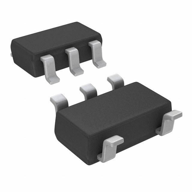
FIN1001
3.3 V LVDS 1-Bit, High-Speed Differential Driver
Features
Description
This single driver is designed for high-speed
interconnects utilizing Low Voltage Differential Signaling
(LVDS) technology. The driver translates LVTTL levels
to LVDS levels with a typical differential output swing of
350 mV which provides low EMI at ultra low power
dissipation even at high frequencies. This device is
ideal for high-speed transfer of clock or data. The
FIN1001 can be paired with its companion receiver, the
FIN1002, or with any other LVDS receiver.
Greater than 600 Mbs Data Rate
3.3 V Power Supply Operation
0.5 ns Maximum Pulse Skew
1.5 ns Maximum Propagation Delay
Low Power Dissipation
Power-Off Protection
Meets or exceeds TIA/EIA-644 LVDS Standard
Flow-through pin-out simplifies PCB Layout
5-Lead SOT23 package saves Space
Ordering Information
Part Number
Operating
Temperature
Range
Package
Packing Method
Packing
Quantity
FIN1001M5X
-40 to +125°C
5-Lead SOT23, JEDEC MO-178, 1.6 mm
Tape & Reel
3000
Connection Diagram
Figure 1. Top View
© 2002 Semiconductor Components Industries, LLC.
FIN1001 • Rev. 1.4
www.fairchildsemi.com
www.onsemi.com
FIN1001 — 3.3V LVDS 1-Bit, High-Speed Differential Driver
March 2017
�Pin #
Name
Description
1
VCC
Power Supply
2
GND
Ground
3
DOUT-
Inverting LVDS Driver Output
4
DOUT+
Non-inverting LVDS Driver Output
5
DIN
LVTTL Data Input
Function Table
Input
Outputs
DIN
DOUT+
DOUT-
LOW
LOW
HIGH
HIGH
HIGH
LOW
Absolute Maximum Ratings
Stresses exceeding the absolute maximum ratings may damage the device. The device may not function or be
operable above the recommended operating conditions and stressing the parts to these levels is not recommended.
In addition, extended exposure to stresses above the recommended operating conditions may affect device
reliability. The absolute maximum ratings are stress ratings only.
Symbol
Parameter
Min.
Max.
Unit
VCC
Supply Voltage
-0.5
4.6
V
DIN
DC Input Voltage
-0.5
6.0
V
DOUT
DC Output Voltage
-0.5
4.6
V
IOSD
Driver Short Circuit Current
16
mA
+150
°C
IO
TSTG
Continuous
Output Current
Storage Temperature Range
-65
TJ
Maximum Junction Temperature
+150
°C
TL
Lead Temperature, Soldering, 10 Seconds
+260
°C
Human Body Model
7500
V
Machine Model
400
V
ESD
Electrostatic Discharge
© 2002 Semiconductor Components Industries, LLC.
FIN1001 • Rev. 1.4
FIN1001 — 3.3V LVDS 1-Bit, High-Speed Differential Driver
Pin Definitions
2
www.fairchildsemi.com
www.onsemi.com
�The Recommended Operating Conditions table defines the conditions for actual device operation. Recommended
operating conditions are specified to ensure optimal performance to the datasheet specifications. ON Semiconductor
does not recommend exceeding them or designing to Absolute Maximum Ratings.
Symbol
Parameter
VCC
Supply Voltage
VIN
Input Voltage
TA
Operating Temperature
Min.
Max.
Unit
3.0
3.6
V
0
VCC
V
-40
+125
°C
DC Electrical Characteristics(1)
All min and max values are guaranteed at TA = -40° to +125°C, unless otherwise specified.
All typical values are at TA = 25°C and with VCC = 3.3 V, unless otherwise specified.
Symbol
VOD
∆VOD
VOS
∆VOS
Parameter
Min
Typ
Max
Unit
TA = -40° to 85°C
250
350
450
mV
TA = -40° to 125°C
230
350
450
mV
25
mV
1.375
V
25
mV
±20
µA
Output Differential Voltage
VOD Magnitude Change from
Differential Low-to-High
RL = 100 Ω,
See Figure 2
Offset Voltage
TA = -40° to 125°C
1.125
1.25
Offset Magnitude Change from
Differential Low-to-High
IOFF
Power-Off Output Current
IOS
Short Circuit Output Current
II(OFF)
Conditions
Power-OFF Input Current
VCC = 0 V,
VOUT = 0 V or 3.6 V
VOUT = 0 V
-5.5
-8
VOD = 0 V
±4
±8
VCC = 0 V, VIN = 0 V or 3.6 V
mA
±20
µA
VIH
Input HIGH Voltage
2.0
VCC
V
VIL
Input LOW Voltage
GND
0.8
V
IIN
Input Current
VIN = 0 V or VCC
±20
µA
Power-Off Input Current
VCC = 0V, VIN = 0 V or 3.6 V
±20
µA
VIK
Input Clamp Voltage
IIK = −18 mA
ICC
Power Supply Current
II(OFF)
CIN
COUT
−1.5
-0.8
FIN1001 — 3.3V LVDS 1-Bit, High-Speed Differential Driver
Recommended Operating Conditions
V
No Load, VIN = 0 V or VCC
4.5
8
RL = 100 Ω, VIN = 0 V or VCC
6.5
10
Input Capacitance
VCC = 3.3 V
3.2
pF
Output Capacitance
VCC = 0 V
3.3
pF
mA
Notes:
1. Not production tested across the full temperature range.
© 2002 Semiconductor Components Industries, LLC.
FIN1001 • Rev. 1.4
3
www.fairchildsemi.com
www.onsemi.com
�AC Electrical Characteristics
All min and max values are guaranteed at TA = -40 to +85°C.
All typical values are at TA = 25°C and with VCC = 3.3 V, unless otherwise specified.
RL = 100 Ω, CL = 5 pF. See Figure 3 and Figure 4.
Symbol
Parameter
Conditions
Min.
Typ.
Max.
Unit
tPLHD
Propagation Delay
LOW to HIGH
0.50
0.98
1.50
ns
tPHLD
Propagation Delay
HIGH to LOW
0.50
0.93
1.50
ns
tTLHD
Differential Output Rise Time
20% to 80%
0.4
0.5
1.0
ns
tTHLD
Output Fall Time
80% to 20%
0.4
0.5
1.0
ns
tSK(p)
Pulse Skew
|tPLH - tPHL|
0.05
0.5
ns
1.0
ns
tSK(PP)
Part-to-Part
Skew(2)
Note:
2. tSK(PP) is the magnitude of the difference in propagation delay times between any specified terminals of two
devices switching in the same direction (either LOW-to-HIGH or HIGH-to-LOW) when both devices operate with
the same supply voltage, same temperature, and have identical test circuits.
© 2002 Semiconductor Components Industries, LLC.
FIN1001 • Rev. 1.4
www.fairchildsemi.com
www.onsemi.com
FIN1001 — 3.3V LVDS 1-Bit, High-Speed Differential Driver
March 2017
�Figure 2. Differential Driver DC Test Circuit
Figure 3. Differential Driver Propagation Delay and
Transition Time Test Circuit
FIN1001 — 3.3V LVDS 1-Bit, High-Speed Differential Driver
Test Diagrams
Figure 4. AC Waveforms
© 2002 Fairchild Semiconductor Corporation
FIN1001 • Rev. 1.4
5
www.fairchildsemi.com
www.onsemi.com
�Figure 5. Output High Voltage vs. Power Supply
Voltage
Figure 6. Output Low Voltage vs. Power Supply
Voltage
Figure 7. Output Short Circuit Current vs. Power
Supply Voltage
Figure 8. Differential Output Voltage vs. Power
Supply Voltage
Figure 9. Differential Output Voltage vs. Load Resistor
Figure 10. Offset Voltage vs. Power Supply
Voltage
© 2002 Fairchild Semiconductor Corporation
FIN1001 • Rev. 1.4
6
FIN1001 — 3.3V LVDS 1-Bit, High-Speed Differential Driver
Typical Performance Characteristics
www.fairchildsemi.com
www.onsemi.com
�Figure 11. Power Supply Current vs. Frequency
Figure 12. Power Supply Current vs. Power Supply
Voltage
5pF
5pF
Figure 13. Power Supply Current vs. Ambient
Temperature
FIN1001 — 3.3V LVDS 1-Bit, High-Speed Differential Driver
Typical Performance Characteristics (Continued)
Figure 14. Differential Propagation Delay vs. Power
Supply
5pF
5pF
Figure 15. Differential Propagation Delay vs. Ambient
Temperature
© 2002 Fairchild Semiconductor Corporation
FIN1001 • Rev. 1.4
Figure 16. Differential Pulse Skew (tPLH - tPHL) vs.
Power Supply Voltage
7
www.fairchildsemi.com
www.onsemi.com
�(Continued)
5pF
5pF
Figure 17. Differential Pulse Skew (tPLH - tPHL) vs.
Ambient Temperature
Figure 18. Transition Time vs. Power Supply
Voltage
5pF
FIN1001 — 3.3V LVDS 1-Bit, High-Speed Differential Driver
Typical Performance Characteristics
Figure 19. Transition Time vs. Ambient Temperature
© 2002 Fairchild Semiconductor Corporation
FIN1001 • Rev. 1.4
8
www.fairchildsemi.com
www.onsemi.com
��ON Semiconductor and
are trademarks of Semiconductor Components Industries, LLC dba ON Semiconductor or its subsidiaries in the United States and/or other countries.
ON Semiconductor owns the rights to a number of patents, trademarks, copyrights, trade secrets, and other intellectual property. A listing of ON Semiconductor’s product/patent
coverage may be accessed at www.onsemi.com/site/pdf/Patent−Marking.pdf. ON Semiconductor reserves the right to make changes without further notice to any products herein.
ON Semiconductor makes no warranty, representation or guarantee regarding the suitability of its products for any particular purpose, nor does ON Semiconductor assume any liability
arising out of the application or use of any product or circuit, and specifically disclaims any and all liability, including without limitation special, consequential or incidental damages.
Buyer is responsible for its products and applications using ON Semiconductor products, including compliance with all laws, regulations and safety requirements or standards,
regardless of any support or applications information provided by ON Semiconductor. “Typical” parameters which may be provided in ON Semiconductor data sheets and/or
specifications can and do vary in different applications and actual performance may vary over time. All operating parameters, including “Typicals” must be validated for each customer
application by customer’s technical experts. ON Semiconductor does not convey any license under its patent rights nor the rights of others. ON Semiconductor products are not
designed, intended, or authorized for use as a critical component in life support systems or any FDA Class 3 medical devices or medical devices with a same or similar classification
in a foreign jurisdiction or any devices intended for implantation in the human body. Should Buyer purchase or use ON Semiconductor products for any such unintended or unauthorized
application, Buyer shall indemnify and hold ON Semiconductor and its officers, employees, subsidiaries, affiliates, and distributors harmless against all claims, costs, damages, and
expenses, and reasonable attorney fees arising out of, directly or indirectly, any claim of personal injury or death associated with such unintended or unauthorized use, even if such
claim alleges that ON Semiconductor was negligent regarding the design or manufacture of the part. ON Semiconductor is an Equal Opportunity/Affirmative Action Employer. This
literature is subject to all applicable copyright laws and is not for resale in any manner.
PUBLICATION ORDERING INFORMATION
LITERATURE FULFILLMENT:
Literature Distribution Center for ON Semiconductor
19521 E. 32nd Pkwy, Aurora, Colorado 80011 USA
Phone: 303−675−2175 or 800−344−3860 Toll Free USA/Canada
Fax: 303−675−2176 or 800−344−3867 Toll Free USA/Canada
Email: orderlit@onsemi.com
© Semiconductor Components Industries, LLC
N. American Technical Support: 800−282−9855 Toll Free
USA/Canada
Europe, Middle East and Africa Technical Support:
Phone: 421 33 790 2910
Japan Customer Focus Center
Phone: 81−3−5817−1050
www.onsemi.com
1
ON Semiconductor Website: www.onsemi.com
Order Literature: http://www.onsemi.com/orderlit
For additional information, please contact your local
Sales Representative
www.onsemi.com
�