Is Now Part of
To learn more about ON Semiconductor, please visit our website at
www.onsemi.com
ON Semiconductor and the ON Semiconductor logo are trademarks of Semiconductor Components Industries, LLC dba ON Semiconductor or its subsidiaries in the United States and/or other countries. ON Semiconductor owns the rights to a number
of patents, trademarks, copyrights, trade secrets, and other intellectual property. A listing of ON Semiconductor’s product/patent coverage may be accessed at www.onsemi.com/site/pdf/Patent-Marking.pdf. ON Semiconductor reserves the right
to make changes without further notice to any products herein. ON Semiconductor makes no warranty, representation or guarantee regarding the suitability of its products for any particular purpose, nor does ON Semiconductor assume any liability
arising out of the application or use of any product or circuit, and specifically disclaims any and all liability, including without limitation special, consequential or incidental damages. Buyer is responsible for its products and applications using ON
Semiconductor products, including compliance with all laws, regulations and safety requirements or standards, regardless of any support or applications information provided by ON Semiconductor. “Typical” parameters which may be provided in ON
Semiconductor data sheets and/or specifications can and do vary in different applications and actual performance may vary over time. All operating parameters, including “Typicals” must be validated for each customer application by customer’s
technical experts. ON Semiconductor does not convey any license under its patent rights nor the rights of others. ON Semiconductor products are not designed, intended, or authorized for use as a critical component in life support systems or any FDA
Class 3 medical devices or medical devices with a same or similar classification in a foreign jurisdiction or any devices intended for implantation in the human body. Should Buyer purchase or use ON Semiconductor products for any such unintended
or unauthorized application, Buyer shall indemnify and hold ON Semiconductor and its officers, employees, subsidiaries, affiliates, and distributors harmless against all claims, costs, damages, and expenses, and reasonable attorney fees arising out
of, directly or indirectly, any claim of personal injury or death associated with such unintended or unauthorized use, even if such claim alleges that ON Semiconductor was negligent regarding the design or manufacture of the part. ON Semiconductor
is an Equal Opportunity/Affirmative Action Employer. This literature is subject to all applicable copyright laws and is not for resale in any manner.
�FJAFS1720
ESBC™ Rated NPN Power Transistor
ESBC Features (FDS8817 MOSFET)
•
•
•
•
•
•
•
Description
VCS(ON)
IC
Equiv. RCS(ON)
0.304 V
10 A
0.0304 Ω (1)
The FJAFS1720 is a low-cost, high-performance power
switch designed to provide the best performance when
used in an ESBC™ configuration in applications such as:
power supplies, motor drivers, smart grid, or ignition
switches. The power switch is designed to operate up to
1700 volts and up to 12 amps, while providing exceptionally low on-resistance and very low switching losses.
Low Equivalent On Resistance
Very Fast Switch: 150 kHz
Squared RBSOA: Up to 1700 V
Avalanche Rated
Low Driving Capacitance, No Miller Capacitance
Low Switching Losses
Reliable HV Switch: No False Triggering due to
High dv/dt Transients
The ESBC™ switch is designed to be driven using off-theshelf power supply controllers or drivers. The ESBC™
MOSFET is a low-voltage, low-cost, surface-mount
device that combines low-input capacitance and fast
switching, The ESBC™ configuration further minimizes
the required driving power because it does not have
Miller capacitance.
Applications
• High-Voltage and High-Speed Power Switches
• Emitter-Switched Bipolar/MOSFET Cascode
(ESBC™)
• Smart Meters, Smart Breakers, SMPS,
HV Industrial Power Supplies
The FJAFS1720 provides exceptional reliability and a
large operating range due to its square reverse-bias-safeoperating-area (RBSOA) and rugged design. The device
is avalanche rated and has no parasitic transistors, so is
not prone to static dv/dt failures.
The power switch is manufactured using a dedicated
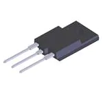
high-voltage bipolar process and is packaged in a highvoltage TO-3PF package.
• Motor Drivers and Ignition Drivers
C
C
2
FJAFS1720
B
1
B
FDS8817
G
TO-3PF
1
1.Base 2.Collector 3.Emitter
Figure 1. Pin Configuration
E
3
S
Figure 2. Internal Schematic Diagram
Figure 3. ESBC Configuration(2)
Ordering Information
Part Number
Marking
Package
Packing Method
FJAFS1720TU
J1720
TO-3PF
TUBE
Notes:
1. Figure of Merit.
2. Other Fairchild MOSFETs can be used in this ESBC application.
© 2012 Fairchild Semiconductor Corporation
FJAFS1720 Rev. 1.0.0
www.fairchildsemi.com
1
FJAFS1720 — ESBC™ Rated NPN Power Transistor
January 2013
�Values are at TA = 25°C unless otherwise noted.
Symbol
VCBO
VCEO
VEBO
IC
PC
TJ
TSTG
Parameter
Collector-Base Voltage
Collector-Emitter Voltage
Emitter-Base Voltage
Collector Current (DC)
Collector Dissipation (TC = 25°C)
Operating and Junction Temperature Range
Storage Temperature Range
Value
Units
1700
800
6
12
60
-55 to +125
-55 to +150
V
V
V
A
W
°C
°C
Max.
Units
2.08
°C/W
Note:
3. Pulse Test is Pulse Width ≤ 5 ms, Duty Cycle ≤ 10%.
Thermal Characteristics
Values are at TA = 25°C unless otherwise noted.
Symbol
RθjC
Parameter
Thermal Resistance, Junction to Case
Electrical Characteristics(4)
Values are at TA = 25°C unless otherwise noted.
Symbol
ICES
ICBO
IEBO
BVCBO
BVCEO
BVEBO
hFE1
hFE2
Parameter
Collector Cut-off Current
Collector Cut-off Current
Emitter Cut-off Current
Collector-Base Breakdown Voltage
Collector-Emitter Breakdown Voltage
Base-Emitter Breakdown Voltage
DC Current Gain
VCE(sat) Collector-Emitter Saturation Voltage
VBE(sat) Base-Emitter Saturation Voltage
Test Conditions
VCB = 1400 V, RBE = 0
VCB = 800 V, IE = 0
VEB = 4 V, IC = 0
IC = 500 μA, IE = 0
IC = 5 mA, IB = 0
IE = 500 μA, IC = 0
VCE = 5 V, IC = 1 A
VCE = 5 V, IC = 11 A
IC = 10 A, IB = 3.33 A, hFE = 3
IC = 5 A, IB = 1.0 A, hFE = 5
IC = 1 A, IB = 0.1 A, hFE = 10
IC = 10 A, IB = 3.33 A, hFE = 3
Min.
Typ. Max. Units
100
10
100
1700
800
6
8.0
5.5
μA
μA
μA
V
V
V
8.5
0.25
0.20
0.20
0.86
V
V
V
V
Note:
4. Pulse Test: Pulse Width ≤ 5 ms, Duty Cycle ≤ 10%.
© 2012 Fairchild Semiconductor Corporation
FJAFS1720 Rev. 1.0.0
www.fairchildsemi.com
2
FJAFS1720 — ESBC™ Rated NPN Power Transistor
Absolute Maximum Ratings(3)
�Values are at TA = 25°C unless otherwise noted.
Symbol
Parameter
fT
Current Gain Bandwidth
Product
Inductive Current Fall Time
Inductive Storage Time
Inductive Voltage Fall Time
Inductive Voltage Rise Time
Inductive Crossover Time
Inductive Current Fall Time
Inductive Storage Time
Inductive Voltage Fall Time
Inductive Voltage Rise Time
Inductive Crossover Time
Maximum Collector Source
Voltage at Turn-off without
Snubber
Gate-Source Leakage Current
Itf
ts
Vtf
Vtr
tc
Itf
ts
Vtf
Vtr
tc
VCSW
IGS(OS)
VCS(ON)
VGS(th)
Ciss
QGS(tot)
rDS(ON)
Collector-Source On Voltage
Gate Threshold Voltage
Input Capacitance
(VGS = VCB = 0)
Gate-Source Charge VCB=0
Static Drain-Source
On Resistance
Test Conditions
Min.
IC = 0.1 A,VCE = 10 V
VGS = 10 V, RG = 47 Ω,
VClamp = 500 V,
IC = 2 A, IB = 0.2 A, hFE = 10
LC = 1 mH,
SRF = 350 kHz
VGS = 10 V, RG = 47 Ω,
VClamp = 500 V,
IC = 5 A, IB = 1 A, hFE = 5
LC = 1 mH,
SRF = 350 kHz
hFE = 5, IC = 6 A
VGS = ±20 V
Typ.
Max. Units
15
MHz
60
1000
85
125
165
24
1500
85
65
110
ns
ns
ns
ns
ns
ns
ns
ns
ns
ns
1700
V
1.0
nA
VGS = 10 V, IC = 10 A, IB = 3.3 A, hFE = 3
0.3040
V
VGS = 10 V, IC = 6 A, IB = 2 A, hFE = 3
0.2124
V
VGS = 10 V, IC = 3 A, IB = 1 A, hFE = 3
0.1362
V
VGS = 10 V, IC = 3 A, IB = 0.6 A, hFE = 5
0.1662
V
VBS = VGS, IB = 250 μA
1.9
V
VCS = 25 V, f = 1 MHz
1805
pF
VGS = 10 V, IC = 6 A, VCS = 25 V
6
nC
VGS = 10 V, ID = 15 A
5.4
mΩ
VGS = 10 V, ID = 15 A, TA = 125 °C
7.5
mΩ
VGS = 4.5 V, ID = 12.6 A
7.0
mΩ
Note:
5. Used typical FDS8817 MOSFET specifications in table. Table could vary if other Fairchild MOSFETs are used.
© 2012 Fairchild Semiconductor Corporation
FJAFS1720 Rev. 1.0.0
www.fairchildsemi.com
3
FJAFS1720 — ESBC™ Rated NPN Power Transistor
ESBC Configured Electrical Characteristics(5)
�16
100
IB=4.0A
VCE = 5V
12
IB=2.0A
10
IB=1.5A
8
IB=1.0A
6
IB=0.2A
o
10
TA = - 25 C
2
0
0
2
4
6
8
1
0.1
10
Figure 4. Static Characteristics
1
100
10
VCE(sat) [V], SATURATION VOLTAGE
IC = 3 IB
o
0.1
TA = 125 C
o
Ta = 25 C
o
TA = - 25 C
0.01
0.1
1
IC = 5 IB
o
TA = 125 C
1
o
TA = 25 C
o
TA = -25 C
0.1
0.01
0.1
10
1
Figure 6. Collector-Emitter Saturation Voltage
hFE=3
Figure 7. Collector-Emitter Saturation Voltage
hFE=5
100
100
VCE(sat) [V], SATURATION VOLTAGE
IC = 10 IB
o
TA = 125 C
o
10
TA = 25 C
o
TA = -25 C
1
0.1
0.1
1
IC = 20 IB
o
TA = -25 C
10
o
TA = 25 C
o
TA = 125 C
1
0.1
0.1
10
IC [A], COLLECTOR CURRENT
1
10
IC [A], COLLECTOR CURRENT
Figure 9. Collector-Emitter Saturation Voltage
hFE=20
Figure 8. Collector-Emitter Saturation Voltage
hFE=10
© 2012 Fairchild Semiconductor Corporation
FJAFS1720 Rev. 1.0.0
10
IC [A], COLLECTOR CURRENT
IC [A], COLLECTOR CURRENT
VCE(sat) [V], SATURATION VOLTAGE
10
Figure 5. DC Current Gain
1
VCE(sat) [V], SATURATION VOLTAGE
TA = 25 C
TA = 125 C
IB=0.5A
4
o
o
hFE, DC CURRENT GAIN
IC [A], COLLECTOR CURRENT
14
www.fairchildsemi.com
4
FJAFS1720 — ESBC™ Rated NPN Power Transistor
Typical Performance Characteristics
�1000
16
IC [A], COLLECTOR CURRENT
14
VCE = 5V
Cob (Emitter Open)
CAPACITANCE [pF]
12
10
8
6
Cob (Emitter Grounded)
Cob (Emitter at socket)
100
4
2
o
125 C
0
0.0
0.2
0.4
o
25 C
o
- 25 C
0.6
0.8
1.0
10
1.2
1
10
100
1000
10000
COLLECTOR-BASE VOLTAGE[V]
VBE [V], BASE-EMITTER VOLTAGE
Figure 10. Base-Emitter On Voltage
Figure 11. Capacitance
160
o
ta = 25 C L=1mH SRF=350KHz
144
o
ta = 25 C L=1mH SRF=350KHz
3.0
hfe=5 common emitter
128
2.5
112
hfe=10 common emitter
hfe=5 common emitter
Time [us]
Time [ns]
96
80
64
hfe=10 common emitter
2.0
1.5
hfe=5 ESBC
hfe=10 ESBC
48
hfe=5 ESBC
32
1.0
hfe=10 ESBC
16
0.5
0
1
2
3
4
5
6
7
8
9
10
11
1
12
2
3
4
5
6
7
8
9
10
11
12
IC [A], COLLECTOR CURRENT
IC [A], COLLECTOR CURRENT
Figure 12. Inductive Load
Collector Current Fall-time (tf)
Figure 13. Inductive Load
Collector Current Storage time (tstg)
440
360
o
ta = 25 C L=1mH SRF=350KHz
400
o
ta = 25 C L=1mH SRF=350KHz
320
360
280
320
240
Time [ns]
Time [ns]
280
240
200
bule line : hfe=10 common emitter
hfe=5 ESBC
hfe=5 common emitter
80
hfe=10 ESBC
120
160
120
hfe=5 common emitter
160
hfe=10 common emitter
200
hfe=5 ESBC
40
80
hfe=10 ESBC
0
40
1
2
3
4
5
6
7
8
9
10
11
1
12
3
4
5
6
7
8
9
10
11
12
IC [A], COLLECTOR CURRENT
IC [A], COLLECTOR CURRENT
Figure 14. Inductive Load
Collector Voltage Fall-time (tf)
Figure 15. Inductive Load
Collector Voltage Rise-time (tr)
© 2012 Fairchild Semiconductor Corporation
FJAFS1720 Rev. 1.0.0
2
www.fairchildsemi.com
5
FJAFS1720 — ESBC™ Rated NPN Power Transistor
Typical Performance Characteristics (Continued)
�400
40
o
ta = 25 C L=1mH SRF=350KHz
360
IC [A], COLLECTOR CURRENT
320
hfe=10 common emitter
280
Time [ns]
RB2 = 0, IB1 = 15A
VCC = 30V, L = 200μH
35
240
200
hfe=5 ESBC
160
hfe=5 common emitter
120
30
25
20
15
VBE(off) = -6V
10
VBE(off) = -3V
5
80
hfe=10 ESBC
1
10
40
1
2
3
4
5
6
7
8
9
10
11
12
IC [A], COLLECTOR CURRENT
1000
10000
VCE [V], COLLECTOR-EMITTER VOLTAGE
Figure 16. Inductive Load
Collector Current / Voltage Crossover (tc)
Figure 17. Reverse Bias Safe Operating Area
100
12
VDD = +/-50V, RLOAD = 500Kohms
IC (Pulse) t = 100ms t = 10ms
HFE = 4
10
IC [A], COLLECTOR CURRENT
IC [A], COLLECTOR CURRENT
100
8
6
4
2
IC (DC)
10
t = 1ms
1
0.1
o
TC = 25 C
Single Pulse
0.01
0
0
200
400
600
800
1000
1200
1400
1600
1
1800
VCE [V], COLLECTOR-EMITTER VOLTAGE
10
100
1000
10000
VCE [V], COLLECTOR-EMITTER VOLTAGE
Figure 18. ESBC RBSOA
Figure 19. Forward Bias Safe Operating Area
PC [W], POWER DISSIPATION
80
60
40
20
0
0
25
50
75
100
125
150
175
O
TC [ C], CASE TEMPERATURE
Figure 20. Power Derating
© 2012 Fairchild Semiconductor Corporation
FJAFS1720 Rev. 1.0.0
www.fairchildsemi.com
6
FJAFS1720 — ESBC™ Rated NPN Power Transistor
Typical Performance Characteristics (Continued)
��
�
�
Figure 21. Test Circuit For Inductive Load and Reverse Bias Safe Operating
}
}
sT
sT
}
pj A
pi
pj A
A
k|{
k|{
R\G}
�
�
�
�
Figure 22. Energy Rating Test Circuit
Figure 24. FBSOA
Figure 23. fT Measurement
© 2012 Fairchild Semiconductor Corporation
FJAFS1720 Rev. 1.0.0
www.fairchildsemi.com
7
FJAFS1720 — ESBC™ Rated NPN Power Transistor
Test Circuits
�FJAFS1720 — ESBC™ Rated NPN Power Transistor
Test Circuits (Continued)
Figure 25. Simplified Saturated Switch Driver Circuit
Functional Test Waveforms
Figure 26. Crossover Time Measurement
toff
90% Vce
90% Ic
10% Vce
10% Ic
Figure 27. Saturated Switching Waveform
© 2012 Fairchild Semiconductor Corporation
FJAFS1720 Rev. 1.0.0
www.fairchildsemi.com
8
�Figure 29. Storage Time - ESBC FET
Gate (off) to IC Fall-Time
Figure 28. Storage Time - Common Emitter
Base turn off (Ib2) to IC Fall-Time
© 2012 Fairchild Semiconductor Corporation
FJAFS1720 Rev. 1.0.0
www.fairchildsemi.com
9
FJAFS1720 — ESBC™ Rated NPN Power Transistor
Functional Test Waveforms (Continued)
�- 80 W; Secondary-Side Regulation: 3 Capacitor Input; Quasi Resonant
24V@3.3A
Y[}gXUY\h
`
X
80 W
ZW~
1YWWTXWWW}Gkj
xGyGXYWro¡
Y
X
Y
|m[WW^
Y^Wr
100kΩ
Z
tiyYWX\Wj{{|
Z
XWWWm
Z\}
XWWWm
Z\}
Y
^
\
[
w]rl[[Wh
twX]W_i[^Xh
680μF
XYWm
[\W}
X
YY}
YL
100kΩ
Y^Wr
FJAFS1720
mqhmzX\XWh{|
Xu[X[_
Y^Wr
100kΩ
}
[\W}
100kΩ
100K
Y^Wr
Q
]
680μF
XYWm
_
FDS8817
mkj]\\
v|{
\
o}
ttzkZW^W
jz
100kΩ
Y^Wr
oXXhnX}t
kl{
X
mi
Y
Z
XYTX[}
XWm
[
XY}¡
[}
680μF
XYWm
[\W}
Xu[X[_~z
100kΩ
Y^Wr
XWWm
Y\}
XUWhG
2.5A
limit
QGtGGG
Driving ESBC Switches
Fairchild
Proprietary
Figure30. VCC Derived
Figure31. Vbias Supply Derived
© 2012 Fairchild Semiconductor Corporation
FJAFS1720 Rev. 1.0.0
Figure32. Proportional Drive
www.fairchildsemi.com
10
FJAFS1720 — ESBC™ Rated NPN Power Transistor
Very Wide Input Voltage Range Supply
�FJAFS1720 — ESBC™ Rated NPN Power Transistor
Physical Dimensions
TO-3PF
15.70
15.30
9.90
4.60
4.40
3.20
2.80
3.80
3.40
7.75
10.20
9.80
16.70
16.30
16.70
16.30
14.70
14.30
1.93
15.00
14.60
23.20
22.80
26.70
26.30
4.20
3.80
1
2
3
2.20
1.80
2.70
2.30
2.20
(3X)
1.80
3.50
3.10
0.95
(3X)
0.65
5.75
5.15
1.10
0.80
5.75
5.15
NOTES:
5.70
5.30
2.20
1.80
3.50
3.10
A. THIS PACKAGE CONFORMS TO SC94
JEITA PACKAGING STANDARD.
B. ALL DIMENSIONS ARE IN MILLIMETERS.
C. DIMENSIONS ARE EXCLUSIVE OF BURRS,
MOLD FLASH AND TIE BAR PROTRUSIONS.
D. PIN 2 CONNECTS TO DAP.
E. DRAWING FILE NAME: TO3PFA03REV1
Figure 33. TO3PF, MOLDED, 3LD, FULLPACK (AG)
Package drawings are provided as a service to customers considering Fairchild components. Drawings may change in any manner
without notice. Please note the revision and/or date on the drawing and contact a Fairchild Semiconductor representative to verify or
obtain the most recent revision. Package specifications do not expand the terms of Fairchild’s worldwide terms and conditions, specifically the
warranty therein, which covers Fairchild products.
Always visit Fairchild Semiconductor’s online packaging area for the most recent package drawings:
http://www.fairchildsemi.com/packaging/.
For current tape and reel specifications, visit Fairchild Semiconductor’s online packaging area:
http://www.fairchildsemi.com/dwg/TO/TO3PFA03.pdf.
© 2012 Fairchild Semiconductor Corporation
FJAFS1720 Rev. 1.0.0
www.fairchildsemi.com
11
�TRADEMARKS
The following includes registered and unregistered trademarks and service marks, owned by Fairchild Semiconductor and/or its global subsidiaries, and is not
intended to be an exhaustive list of all such trademarks.
FPS¥
F-PFS¥
FRFET®
SM
Global Power Resource
GreenBridge¥
Green FPS¥
Green FPS¥ e-Series¥
Gmax¥
GTO¥
IntelliMAX¥
ISOPLANAR¥
Making Small Speakers Sound Louder
and Better™
MegaBuck¥
MICROCOUPLER¥
MicroFET¥
MicroPak¥
MicroPak2¥
MillerDrive¥
MotionMax¥
mWSaver¥
OptoHiT¥
OPTOLOGIC®
OPTOPLANAR®
2Cool¥
AccuPower¥
AX-CAP®*
BitSiC¥
Build it Now¥
CorePLUS¥
CorePOWER¥
CROSSVOLT¥
CTL¥
Current Transfer Logic¥
DEUXPEED®
Dual Cool™
EcoSPARK®
EfficientMax¥
ESBC¥
®
Fairchild®
Fairchild Semiconductor®
FACT Quiet Series¥
FACT®
FAST®
FastvCore¥
FETBench¥
Sync-Lock™
®
PowerTrench®
PowerXS™
Programmable Active Droop¥
QFET®
QS¥
Quiet Series¥
RapidConfigure¥
¥
Saving our world, 1mW/W/kW at a time™
SignalWise¥
SmartMax¥
SMART START¥
Solutions for Your Success¥
SPM®
STEALTH¥
SuperFET®
SuperSOT¥-3
SuperSOT¥-6
SuperSOT¥-8
SupreMOS®
SyncFET¥
®*
TinyBoost¥
TinyBuck¥
TinyCalc¥
TinyLogic®
TINYOPTO¥
TinyPower¥
TinyPWM¥
TinyWire¥
TranSiC¥
TriFault Detect¥
TRUECURRENT®*
PSerDes¥
UHC®
Ultra FRFET¥
UniFET¥
VCX¥
VisualMax¥
VoltagePlus¥
XS™
* Trademarks of System General Corporation, used under license by Fairchild Semiconductor.
DISCLAIMER
FAIRCHILD SEMICONDUCTOR RESERVES THE RIGHT TO MAKE CHANGES WITHOUT FURTHER NOTICE TO ANY PRODUCTS HEREIN TO IMPROVE
RELIABILITY, FUNCTION, OR DESIGN. FAIRCHILD DOES NOT ASSUME ANY LIABILITY ARISING OUT OF THE APPLICATION OR USE OF ANY PRODUCT
OR CIRCUIT DESCRIBED HEREIN; NEITHER DOES IT CONVEY ANY LICENSE UNDER ITS PATENT RIGHTS, NOR THE RIGHTS OF OTHERS. THESE
SPECIFICATIONS DO NOT EXPAND THE TERMS OF FAIRCHILD’S WORLDWIDE TERMS AND CONDITIONS, SPECIFICALLY THE WARRANTY THEREIN,
WHICH COVERS THESE PRODUCTS.
LIFE SUPPORT POLICY
FAIRCHILD’S PRODUCTS ARE NOT AUTHORIZED FOR USE AS CRITICAL COMPONENTS IN LIFE SUPPORT DEVICES OR SYSTEMS WITHOUT THE
EXPRESS WRITTEN APPROVAL OF FAIRCHILD SEMICONDUCTOR CORPORATION.
As used herein:
1. Life support devices or systems are devices or systems which, (a) are
2. A critical component in any component of a life support, device, or
system whose failure to perform can be reasonably expected to
intended for surgical implant into the body or (b) support or sustain
life, and (c) whose failure to perform when properly used in
cause the failure of the life support device or system, or to affect its
accordance with instructions for use provided in the labeling, can be
safety or effectiveness.
reasonably expected to result in a significant injury of the user.
ANTI-COUNTERFEITING POLICY
Fairchild Semiconductor Corporation's Anti-Counterfeiting Policy. Fairchild's Anti-Counterfeiting Policy is also stated on our external website, www.fairchildsemi.com,
under Sales Support.
Counterfeiting of semiconductor parts is a growing problem in the industry. All manufacturers of semiconductor products are experiencing counterfeiting of their
parts. Customers who inadvertently purchase counterfeit parts experience many problems such as loss of brand reputation, substandard performance, failed
applications, and increased cost of production and manufacturing delays. Fairchild is taking strong measures to protect ourselves and our customers from the
proliferation of counterfeit parts. Fairchild strongly encourages customers to purchase Fairchild parts either directly from Fairchild or from Authorized Fairchild
Distributors who are listed by country on our web page cited above. Products customers buy either from Fairchild directly or from Authorized Fairchild Distributors
are genuine parts, have full traceability, meet Fairchild's quality standards for handling and storage and provide access to Fairchild's full range of up-to-date technical
and product information. Fairchild and our Authorized Distributors will stand behind all warranties and will appropriately address any warranty issues that may arise.
Fairchild will not provide any warranty coverage or other assistance for parts bought from Unauthorized Sources. Fairchild is committed to combat this global
problem and encourage our customers to do their part in stopping this practice by buying direct or from authorized distributors.
PRODUCT STATUS DEFINITIONS
Definition of Terms
Datasheet Identification
Product Status
Advance Information
Formative / In Design
Preliminary
First Production
No Identification Needed
Full Production
Obsolete
Not In Production
Definition
Datasheet contains the design specifications for product development. Specifications may change
in any manner without notice.
Datasheet contains preliminary data; supplementary data will be published at a later date. Fairchild
Semiconductor reserves the right to make changes at any time without notice to improve design.
Datasheet contains final specifications. Fairchild Semiconductor reserves the right to make
changes at any time without notice to improve the design.
Datasheet contains specifications on a product that is discontinued by Fairchild Semiconductor.
The datasheet is for reference information only.
Rev. I64
© Fairchild Semiconductor Corporation
www.fairchildsemi.com
�ON Semiconductor and
are trademarks of Semiconductor Components Industries, LLC dba ON Semiconductor or its subsidiaries in the United States and/or other countries.
ON Semiconductor owns the rights to a number of patents, trademarks, copyrights, trade secrets, and other intellectual property. A listing of ON Semiconductor’s product/patent
coverage may be accessed at www.onsemi.com/site/pdf/Patent−Marking.pdf. ON Semiconductor reserves the right to make changes without further notice to any products herein.
ON Semiconductor makes no warranty, representation or guarantee regarding the suitability of its products for any particular purpose, nor does ON Semiconductor assume any liability
arising out of the application or use of any product or circuit, and specifically disclaims any and all liability, including without limitation special, consequential or incidental damages.
Buyer is responsible for its products and applications using ON Semiconductor products, including compliance with all laws, regulations and safety requirements or standards,
regardless of any support or applications information provided by ON Semiconductor. “Typical” parameters which may be provided in ON Semiconductor data sheets and/or
specifications can and do vary in different applications and actual performance may vary over time. All operating parameters, including “Typicals” must be validated for each customer
application by customer’s technical experts. ON Semiconductor does not convey any license under its patent rights nor the rights of others. ON Semiconductor products are not
designed, intended, or authorized for use as a critical component in life support systems or any FDA Class 3 medical devices or medical devices with a same or similar classification
in a foreign jurisdiction or any devices intended for implantation in the human body. Should Buyer purchase or use ON Semiconductor products for any such unintended or unauthorized
application, Buyer shall indemnify and hold ON Semiconductor and its officers, employees, subsidiaries, affiliates, and distributors harmless against all claims, costs, damages, and
expenses, and reasonable attorney fees arising out of, directly or indirectly, any claim of personal injury or death associated with such unintended or unauthorized use, even if such
claim alleges that ON Semiconductor was negligent regarding the design or manufacture of the part. ON Semiconductor is an Equal Opportunity/Affirmative Action Employer. This
literature is subject to all applicable copyright laws and is not for resale in any manner.
PUBLICATION ORDERING INFORMATION
LITERATURE FULFILLMENT:
Literature Distribution Center for ON Semiconductor
19521 E. 32nd Pkwy, Aurora, Colorado 80011 USA
Phone: 303−675−2175 or 800−344−3860 Toll Free USA/Canada
Fax: 303−675−2176 or 800−344−3867 Toll Free USA/Canada
Email: orderlit@onsemi.com
© Semiconductor Components Industries, LLC
N. American Technical Support: 800−282−9855 Toll Free
USA/Canada
Europe, Middle East and Africa Technical Support:
Phone: 421 33 790 2910
Japan Customer Focus Center
Phone: 81−3−5817−1050
www.onsemi.com
1
ON Semiconductor Website: www.onsemi.com
Order Literature: http://www.onsemi.com/orderlit
For additional information, please contact your local
Sales Representative
www.onsemi.com
�