Is Now Part of
To learn more about ON Semiconductor, please visit our website at
www.onsemi.com
Please note: As part of the Fairchild Semiconductor integration, some of the Fairchild orderable part numbers
will need to change in order to meet ON Semiconductor’s system requirements. Since the ON Semiconductor
product management systems do not have the ability to manage part nomenclature that utilizes an underscore
(_), the underscore (_) in the Fairchild part numbers will be changed to a dash (-). This document may contain
device numbers with an underscore (_). Please check the ON Semiconductor website to verify the updated
device numbers. The most current and up-to-date ordering information can be found at www.onsemi.com. Please
email any questions regarding the system integration to Fairchild_questions@onsemi.com.
ON Semiconductor and the ON Semiconductor logo are trademarks of Semiconductor Components Industries, LLC dba ON Semiconductor or its subsidiaries in the United States and/or other countries. ON Semiconductor owns the rights to a number
of patents, trademarks, copyrights, trade secrets, and other intellectual property. A listing of ON Semiconductor’s product/patent coverage may be accessed at www.onsemi.com/site/pdf/Patent-Marking.pdf. ON Semiconductor reserves the right
to make changes without further notice to any products herein. ON Semiconductor makes no warranty, representation or guarantee regarding the suitability of its products for any particular purpose, nor does ON Semiconductor assume any liability
arising out of the application or use of any product or circuit, and specifically disclaims any and all liability, including without limitation special, consequential or incidental damages. Buyer is responsible for its products and applications using ON
Semiconductor products, including compliance with all laws, regulations and safety requirements or standards, regardless of any support or applications information provided by ON Semiconductor. “Typical” parameters which may be provided in ON
Semiconductor data sheets and/or specifications can and do vary in different applications and actual performance may vary over time. All operating parameters, including “Typicals” must be validated for each customer application by customer’s
technical experts. ON Semiconductor does not convey any license under its patent rights nor the rights of others. ON Semiconductor products are not designed, intended, or authorized for use as a critical component in life support systems or any FDA
Class 3 medical devices or medical devices with a same or similar classification in a foreign jurisdiction or any devices intended for implantation in the human body. Should Buyer purchase or use ON Semiconductor products for any such unintended
or unauthorized application, Buyer shall indemnify and hold ON Semiconductor and its officers, employees, subsidiaries, affiliates, and distributors harmless against all claims, costs, damages, and expenses, and reasonable attorney fees arising out
of, directly or indirectly, any claim of personal injury or death associated with such unintended or unauthorized use, even if such claim alleges that ON Semiconductor was negligent regarding the design or manufacture of the part. ON Semiconductor
is an Equal Opportunity/Affirmative Action Employer. This literature is subject to all applicable copyright laws and is not for resale in any manner.
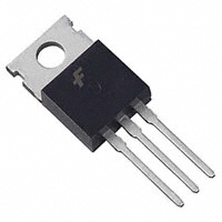
�FJP5027
FJP5027
High Voltage and High Reliability
• High Speed Switching
• Wide SOA
TO-220
1
1.Base
2.Collector
3.Emitter
NPN Silicon Transistor
Absolute Maximum Ratings TC=25°C unless otherwise noted
Symbol
VCBO
Parameter
Collector-Base Voltage
Value
1100
Units
V
800
V
VCEO
Collector-Emitter Voltage
VEBO
Emitter-Base Voltage
7
V
IC
Collector Current (DC)
3
A
A
ICP
Collector Current (Pulse)
10
IB
Base Current
1.5
A
PC
Collector Dissipation ( TC=25°C)
50
W
TJ
Junction Temperature
150
°C
TSTG
Storage Temperature
- 55 ~ 150
°C
Electrical Characteristics TC=25°C unless otherwise noted
Symbol
BVCBO
Parameter
Collector-Base Breakdown Voltage
Test Condition
IC = 1mA, IE = 0
BVCEO
Collector-Emitter Breakdown Voltage
IC = 5mA, IB = 0
800
BVEBO
Emitter-Base Breakdown Voltage
IE = 1mA, IC = 0
7
V
VCEX(sus)
Collector-Emitter Sustaining Voltage
IC = 1.5A, IB1 = -IB2 = 0.3A
L = 2mH, Clamped
800
V
ICBO
Collector Cut-off Current
VCB = 800V, IE = 0
10
µA
IEBO
Emitter Cut-off Current
VEB = 5V, IC = 0
10
µA
hFE1
hFE2
DC Current Gain
VCE = 5V, IC = 0.2A
VCE = 5V, IC = 1A
VCE(sat)
Collector-Emitter Saturation Voltage
IC = 1.5A, IB = 0.3A
2
V
VBE(sat)
Base-Emitter Saturation Voltage
IC = 1.5A, IB = 0.3A
1.5
V
Cob
Output Capacitance
VCB = 10V, IE = 0, f = 1MHz
60
pF
fT
Current Gain Bandwidth Product
VCE = 10V, IC = 0.2A
15
MHz
VCC = 400V
IC = 5IB1 = -2.5IB2 = 2A
RL = 200Ω
tON
Turn On Time
tSTG
Storage Time
tF
Fall Time
Min.
1100
Typ.
Max.
Units
V
V
10
8
40
0.5
µs
3
µs
0.3
µs
hFE Classification
Classification
N
R
O
hFE1
10 ~ 20
15 ~ 30
20 ~ 40
©2003 Fairchild Semiconductor Corporation
Rev. A, December 2003
�FJP5027
Typical Characteristics
3.0
100
VCE = 5 V
IB = 350mA
2.5
IC [A], COLLECTOR CURRENT
o
o
hFE, DC CURRENT GAIN
TC = 125 C
2.0
IB = 150mA
1.5
IB = 100mA
1.0
IB = 50mA
TC = 75 C
o
TC = - 25 C
o
TC = 25 C
10
0.5
0.0
0
1
2
3
4
5
6
7
1
0.01
8
0.1
Figure 1. Static Characteristic
10
Figure 2. DC current Gain
100
10
IC = 5 IB
VBE(sat) [V], SATURATION VOLTAGE
VCE(sat) [V], SATURATION VOLTAGE
1
IC [A], COLLECTOR CURRENT
VCE [V], COLLECTOR-EMITTER VOLTAGE
o
TC = 125 C
10
o
TC = 75 C
o
TC = 25 C
1
o
TC = - 25 C
0.1
0.01
0.1
1
IC = 5 IB
o
TC = 25 C
1
o
TC = - 25 C
o
o
TC = 125 C
TC = 75 C
0.1
0.1
10
IC [A], COLLECTOR CURRENT
1
10
IC [A], COLLECTOR CURRENT
Figure 3. Base-Emitter Saturation Voltage
Collector-Emitter Saturation Voltage
Figure 4. Base-Emitter On Voltage
IC[A], COLLECTOR CURRENT
IC [A], COLLECTOR CURRENT
100
10
IB1=3A, RB2=0
L=1mH, VCC=20V
1
10
100
1000
ICMAX.(Pulse)
10
ICMAX(Continuous)
10ms
1ms
100µs
DC
1
0.1
0.01
1E-3
1
10
100
1000
10000
VCE [V], COLLECTOR-EMITTER VOLTAGE
VCE[V], COLLECTOR-EMITTER VOLTAGE
Figure 5. Switching Time
©2003 Fairchild Semiconductor Corporation
Figure 6. Safe Operating Area
Rev. A, December 2003
�FJP5027
Typical Characteristics (Continued)
80
10
PC[W], POWER DISSIPATION
tF, tSTG [µ s], SWITCHING TIME
70
1
0.1
IB1=45mA, IB2=-0.5A
VCC=125V
60
50
40
30
20
10
0
0.01
0.1
1
10
IC [A], COLLECTOR CURRENT
Figure 7. Resistive Load Switching Characteristics
©2003 Fairchild Semiconductor Corporation
0
25
50
75
100
125
150
175
o
TC[ C], CASE TEMPERATURE
Figure 8. Power Derating
Rev. A, December 2003
�SUPPLIER "B" PACKAGE
SHAPE
3.50
10.67
9.65 E
SUPPLIER "A" PACKAGE
SHAPE
3.40
2.50
16.30
13.90
IF PRESENT, SEE NOTE "D"
16.51
15.42
E
9.40
8.13 E
1
[2.46]
2
3
C
4.10
2.70
14.04
12.70
2.13
2.06
FRONT VIEWS
4.70
4.00
1.62 H
1.42
"A1"
8.65
7.59
SEE NOTE "F"
1.62
1.10
2.67
2.40
1.00
0.55
6.69
6.06
OPTIONAL
CHAMFER
E
14.30
11.50
NOTE "I"
BOTTOM VIEW
3
0.60
0.36
SIDE VIEW
2.85
2.10
2
1
BACK VIEW
NOTES:
A) REFERENCE JEDEC, TO-220, VARIATION AB
B) ALL DIMENSIONS ARE IN MILLIMETERS.
C) DIMENSIONS COMMON TO ALL PACKAGE
SUPPLIERS EXCEPT WHERE NOTED [ ].
D) LOCATION OF MOLDED FEATURE MAY VARY
(LOWER LEFT CORNER, LOWER CENTER
AND CENTER OF THE PACKAGE)
E DOES NOT COMPLY JEDEC STANDARD VALUE.
F) "A1" DIMENSIONS AS BELOW:
SINGLE GAUGE = 0.51 - 0.61
DUAL GAUGE = 1.10 - 1.45
G) DRAWING FILE NAME: TO220B03REV9
H PRESENCE IS SUPPLIER DEPENDENT
I) SUPPLIER DEPENDENT MOLD LOCKING HOLES
IN HEATSINK.
�ON Semiconductor and
are trademarks of Semiconductor Components Industries, LLC dba ON Semiconductor or its subsidiaries in the United States and/or other countries.
ON Semiconductor owns the rights to a number of patents, trademarks, copyrights, trade secrets, and other intellectual property. A listing of ON Semiconductor’s product/patent
coverage may be accessed at www.onsemi.com/site/pdf/Patent−Marking.pdf. ON Semiconductor reserves the right to make changes without further notice to any products herein.
ON Semiconductor makes no warranty, representation or guarantee regarding the suitability of its products for any particular purpose, nor does ON Semiconductor assume any liability
arising out of the application or use of any product or circuit, and specifically disclaims any and all liability, including without limitation special, consequential or incidental damages.
Buyer is responsible for its products and applications using ON Semiconductor products, including compliance with all laws, regulations and safety requirements or standards,
regardless of any support or applications information provided by ON Semiconductor. “Typical” parameters which may be provided in ON Semiconductor data sheets and/or
specifications can and do vary in different applications and actual performance may vary over time. All operating parameters, including “Typicals” must be validated for each customer
application by customer’s technical experts. ON Semiconductor does not convey any license under its patent rights nor the rights of others. ON Semiconductor products are not
designed, intended, or authorized for use as a critical component in life support systems or any FDA Class 3 medical devices or medical devices with a same or similar classification
in a foreign jurisdiction or any devices intended for implantation in the human body. Should Buyer purchase or use ON Semiconductor products for any such unintended or unauthorized
application, Buyer shall indemnify and hold ON Semiconductor and its officers, employees, subsidiaries, affiliates, and distributors harmless against all claims, costs, damages, and
expenses, and reasonable attorney fees arising out of, directly or indirectly, any claim of personal injury or death associated with such unintended or unauthorized use, even if such
claim alleges that ON Semiconductor was negligent regarding the design or manufacture of the part. ON Semiconductor is an Equal Opportunity/Affirmative Action Employer. This
literature is subject to all applicable copyright laws and is not for resale in any manner.
PUBLICATION ORDERING INFORMATION
LITERATURE FULFILLMENT:
Literature Distribution Center for ON Semiconductor
19521 E. 32nd Pkwy, Aurora, Colorado 80011 USA
Phone: 303−675−2175 or 800−344−3860 Toll Free USA/Canada
Fax: 303−675−2176 or 800−344−3867 Toll Free USA/Canada
Email: orderlit@onsemi.com
© Semiconductor Components Industries, LLC
N. American Technical Support: 800−282−9855 Toll Free
USA/Canada
Europe, Middle East and Africa Technical Support:
Phone: 421 33 790 2910
Japan Customer Focus Center
Phone: 81−3−5817−1050
www.onsemi.com
1
ON Semiconductor Website: www.onsemi.com
Order Literature: http://www.onsemi.com/orderlit
For additional information, please contact your local
Sales Representative
www.onsemi.com
�