Is Now Part of
To learn more about ON Semiconductor, please visit our website at
www.onsemi.com
Please note: As part of the Fairchild Semiconductor integration, some of the Fairchild orderable part numbers
will need to change in order to meet ON Semiconductor’s system requirements. Since the ON Semiconductor
product management systems do not have the ability to manage part nomenclature that utilizes an underscore
(_), the underscore (_) in the Fairchild part numbers will be changed to a dash (-). This document may contain
device numbers with an underscore (_). Please check the ON Semiconductor website to verify the updated
device numbers. The most current and up-to-date ordering information can be found at www.onsemi.com. Please
email any questions regarding the system integration to Fairchild_questions@onsemi.com.
ON Semiconductor and the ON Semiconductor logo are trademarks of Semiconductor Components Industries, LLC dba ON Semiconductor or its subsidiaries in the United States and/or other countries. ON Semiconductor owns the rights to a number
of patents, trademarks, copyrights, trade secrets, and other intellectual property. A listing of ON Semiconductor’s product/patent coverage may be accessed at www.onsemi.com/site/pdf/Patent-Marking.pdf. ON Semiconductor reserves the right
to make changes without further notice to any products herein. ON Semiconductor makes no warranty, representation or guarantee regarding the suitability of its products for any particular purpose, nor does ON Semiconductor assume any liability
arising out of the application or use of any product or circuit, and specifically disclaims any and all liability, including without limitation special, consequential or incidental damages. Buyer is responsible for its products and applications using ON
Semiconductor products, including compliance with all laws, regulations and safety requirements or standards, regardless of any support or applications information provided by ON Semiconductor. “Typical” parameters which may be provided in ON
Semiconductor data sheets and/or specifications can and do vary in different applications and actual performance may vary over time. All operating parameters, including “Typicals” must be validated for each customer application by customer’s
technical experts. ON Semiconductor does not convey any license under its patent rights nor the rights of others. ON Semiconductor products are not designed, intended, or authorized for use as a critical component in life support systems or any FDA
Class 3 medical devices or medical devices with a same or similar classification in a foreign jurisdiction or any devices intended for implantation in the human body. Should Buyer purchase or use ON Semiconductor products for any such unintended
or unauthorized application, Buyer shall indemnify and hold ON Semiconductor and its officers, employees, subsidiaries, affiliates, and distributors harmless against all claims, costs, damages, and expenses, and reasonable attorney fees arising out
of, directly or indirectly, any claim of personal injury or death associated with such unintended or unauthorized use, even if such claim alleges that ON Semiconductor was negligent regarding the design or manufacture of the part. ON Semiconductor
is an Equal Opportunity/Affirmative Action Employer. This literature is subject to all applicable copyright laws and is not for resale in any manner.
�Motion-SPM
FNA40860/B2
TM
Smart Power Module
Features
General Description
• 600V-8A 3-phase IGBT inverter bridge including control ICs
for gate driving and protection
It is an advanced motion-smart power module (Motion-SPMTM)
that Fairchild has newly developed and designed to provide
very compact and high performance ac motor drives mainly targeting low-power inverter-driven application like air conditioner
and refrigerator. It combines optimized circuit protection and
drive matched to low-loss IGBTs. System reliability is further
enhanced by the integrated under-voltage lock-out protection,
short-circuit protection, and temperature monitoring. The high
speed built-in HVIC provides opto-coupler-less single-supply
IGBT gate driving capability that further reduce the overall size
of the inverter system design. Each phase current of inverter
can be monitored separately due to the divided negative dc terminals.
• Easy PCB layout due to built-in bootstrap diode and VS output
• Divided negative dc-link terminals for inverter current sensing
applications
• Single-grounded power supply due to built-in HVIC
• Built-in thermistor for over-temperature monitoring
• Isolation rating of 2000Vrms/min.
Applications
Additional Information
• AC 100V ~ 253V three-phase inverter drive for small power
ac motor drives
For further infomation, please see AN-9070 and FEB305-001 in
http://www.fairchildsemi.com
• Home appliances applications like air conditioner and refrigerator
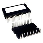
Figure 1.
©2011 Fairchild Semiconductor Corporation
FNA40860/B2 Rev. C
1
www.fairchildsemi.com
FNA40860/B2 Smart Power Module ( Daikin only )
June 2011
�FNA40860/B2 Smart Power Module ( Daikin only )
Integrated Power Functions
• 600V-8A IGBT inverter for three-phase DC/AC power conversion (Please refer to Figure 3)
Integrated Drive, Protection and System Control Functions
• For inverter high-side IGBTs: Gate drive circuit, High voltage isolated high-speed level shifting
Control circuit under-voltage (UV) protection
• For inverter low-side IGBTs: Gate drive circuit, Short circuit protection (SC)
Control supply circuit under-voltage (UV) protection
• Fault signaling: Corresponding to UV (Low-side supply) and SC faults
• Input interface: 3.3/5V CMOS compatible, Schmitt trigger input
Pin Configuration
Top View
VB(U) (26)
V TH(1)
VS(U)(25)
R TH(2)
VB(V)(24)
V S(V)(23)
P(3)
V B(W)(22)
VS(W)(21)
U(4)
IN (UH) (20)
Case Temperature (TC)
Detecting Point
IN(VH)(19)
V(5)
IN(WH)(18)
VCC(H) (17)
VCC(L)(16)
W(6)
COM(15)
IN (UL)(14)
IN (VL)(13)
N U(7)
IN (WL) (12)
N V(8)
VFO (11)
NW(9)
CSC(10)
Figure 2.
FNA40860/B2 Rev. C
2
www.fairchildsemi.com
�FNA40860/B2 Smart Power Module ( Daikin only )
Pin Descriptions
Pin Number
Pin Name
1
V TH
Pin Description
Thermistor Bias Voltage
2
RTH
3
P
Series Resistor for the Use of Thermistor (Temperature Detection)
4
U
Output for U Phase
5
V
Output for V Phase
6
W
Output for W Phase
7
NU
Negative DC–Link Input for U Phase
Positive DC–Link Input
8
NV
Negative DC–Link Input for V Phase
9
NW
Negative DC–Link Input for W Phase
10
CSC
Capacitor (Low-pass Filter) for Short-Current Detection Input
11
VFO
Fault Output
12
IN(WL)
Signal Input for Low-side W Phase
13
IN (VL)
Signal Input for Low-side V Phase
14
IN(UL)
Signal Input for Low-side U Phase
15
COM
Common Supply Ground
16
VCC(L)
Low-Side Common Bias Voltage for IC and IGBTs Driving
17
V CC(H)
High-Side Common Bias Voltage for IC and IGBTs Driving
18
IN(WH)
Signal Input for High-side W Phase
19
IN (VH)
Signal Input for High-side V Phase
20
IN(UH)
Signal Input for High-side U Phase
21
VS(W)
High-side Bias Voltage Ground for W Phase IGBT Driving
22
VB(W)
High-side Bias Voltage for W Phase IGBT Driving
23
V S(V)
High-side Bias Voltage Ground for V Phase IGBT Driving
24
V B(V)
High-side Bias Voltage for V Phase IGBT Driving
25
VS(U)
High-side Bias Voltage Ground for U Phase IGBT Driving
26
VB(U)
High-side Bias Voltage for U Phase IGBT Driving
FNA40860/B2 Rev. C
3
www.fairchildsemi.com
�FNA40860/B2 Smart Power Module ( Daikin only )
Internal Equivalent Circuit and Input/Output Pins
VTH (1)
Thermister
(26) VB(U)
(25) VS(U)
(24) VB(V)
(23) VS(V)
(22) VB(W)
(21) VS(W)
(20) IN(UH)
(19) IN(VH)
(18) IN(WH)
(17) VCC(H)
(16) VCC(L)
(15) COM
(14) IN(UL)
(13) IN(VL)
(12) IN(WL)
(11) VFO
(10) CSC
RTH (2)
P (3)
UVB
UVS
VVB
OUT(UH)
UVS
U(4)
VVS
WVB
WVS
IN(UH)
OUT(VH)
VVS
V (5)
IN(VH)
IN(WH)
VCC
OUT(WH)
COM
WVS
W(6)
VCC
OUT(UL)
COM
NU (7)
IN(UL)
IN(VL)
IN(WL)
OUT(VL)
NV (8)
VFO
C(SC)
OUT(WL)
NW (9)
Note:
1) Inverter high-side is composed of three IGBTs, freewheeling diodes and one control IC for each IGBT.
2) Inverter low-side is composed of three IGBTs, freewheeling diodes and one control IC for each IGBT. It has gate drive and protection functions.
3) Inverter power side is composed of four inverter dc-link input terminals and three inverter output terminals.
Figure 3.
FNA40860/B2 Rev. C
4
www.fairchildsemi.com
�Unless Otherwise Specified)
Inverter Part
Symbol
VPN
V PN(Surge)
VCES
Parameter
Conditions
Rating
Units
Supply Voltage
Applied between P- NU, NV, NW
450
V
Supply Voltage (Surge)
Applied between P- NU, NV, NW
500
V
600
V
Collector-emitter Voltage
± IC
Each IGBT Collector Current
TC = 25°C, TJ < 150°C
8
A
± ICP
Each IGBT Collector Current (Peak)
TC = 25°C, TJ < 150°C, V PN = 300V, Under
1ms Pulse Width
24
A
PC
Collector Dissipation
TC = 25°C per One Chip
32
W
TJ
Operating Junction Temperature
(Note 1)
-40 ~ 150
°C
Rating
Units
Note:
1. The maximum junction temperature rating of the power chips integrated within the SPM is 150°C.
Control Part
Symbol
Parameter
Conditions
VCC
Control Supply Voltage
Applied between V CC(H), VCC(L) - COM
20
V
VBS
High-side Control Bias
Voltage
Applied between V B(U) - VS(U), VB(V) - VS(V),
VB(W) - V S(W)
20
V
VIN
Input Signal Voltage
Applied between IN(UH), IN(VH), IN(WH), -0.3~VCC +0.3
IN(UL), IN(VL), IN(WL) - COM
V
VFO
Fault Output Supply Voltage
Applied between V FO - COM
-0.3~VCC +0.3
V
IFO
Fault Output Current
Sink Current at V FO Pin
VSC
Current Sensing Input Voltage
Applied between C SC - COM
1
mA
-0.3~VCC +0.3
V
Rating
Units
600
V
0.5
A
Bootstrap Diode Part
Symbol
VRRM
IF
Parameter
Conditions
Maximum Repetitive Reverse Voltage
Forward Current
TC = 25°C
IFP
Forward Current (Peak)
TC = 25°C, Under 1ms Pulse Width
TJ
Operating Junction Temperature
1
A
-40 ~ 150
°C
Rating
Units
400
V
Total System
Symbol
VPN(PROT)
Parameter
Self Protection Supply Voltage Limit
(Short Circuit Protection Capability)
TSTG
Storage Temperature
V ISO
Isolation Voltage
Conditions
VCC = VBS = 13.5 ~ 16.5V
TJ = 150°C, Non-repetitive, less than 2ms
60Hz, Sinusoidal, AC 1 minute, Connection
Pins to heat sink plate
-40 ~ 125
°C
2000
Vrms
Thermal Resistance
Symbol
Rth(j-c)Q
Rth(j-c)F
Parameter
Junction to Case Thermal
Resistance
Conditions
Min.
Typ. Max. Units
Inverter IGBT part (per 1/6 module)
-
-
3.8
°C/W
Inverter FWD part (per 1/6 module)
-
-
4.8
°C/W
Note:
2. For the measurement point of case temperature(TC), please refer to Figure 2.
FNA40860/B2 Rev. C
5
www.fairchildsemi.com
FNA40860/B2 Smart Power Module ( Daikin only )
Absolute Maximum Ratings (TJ = 25°C,
�Inverter Part
Symbol
Parameter
VCE(SAT)
Collector-Emitter Saturation
Voltage
VCC = VBS = 15V
VIN = 5V
FWD Forward Voltage
VIN = 0V
Switching Times
VPN = 300V, V CC = VBS = 15V, IC = 8A
TJ = 25°C
VIN = 0V « 5V, Inductive Load
(Note 3)
VF
HS
tON
Conditions
tC(ON)
tOFF
Min.
Typ.
IC = 8A, TJ = 25°C
-
1.7
2.2
V
IF = 8A, TJ = 25°C
-
1.7
2.2
V
0.45
0.75
1.25
ms
-
0.20
0.45
ms
-
0.80
1.30
ms
-
0.30
0.55
ms
-
0.15
-
ms
0.45
0.75
1.25
ms
tC(OFF)
trr
LS
tON
VPN = 300V, V CC = VBS = 15V, IC = 8A
TJ = 25°C
VIN = 0V « 5V, Inductive Load
(Note 3)
Max. Units
-
0.20
0.45
ms
-
0.80
1.30
ms
tC(OFF)
-
0.30
0.55
ms
trr
-
0.15
-
ms
-
-
1
mA
tC(ON)
tOFF
ICES
Collector-Emitter
Leakage Current
VCE = VCES
Note:
3. tON and tOFF include the propagation delay time of the internal drive IC. tC(ON) and tC(OFF) are the switching time of IGBT itself under the given gate driving condition internally.
For the detailed information, please see Figure 4.
100% IC 100% IC
t rr
V CE
IC
IC
V IN
V IN
t ON
10% IC
V IN(ON )
V CE
tO FF
tC(O N)
90% IC
t C(OFF)
V IN (OF F)
10% V C E
10% V C E
10% I C
(b) turn-off
(a) turn-on
Figure 4. Switching Time Definition
FNA40860/B2 Rev. C
6
www.fairchildsemi.com
FNA40860/B2 Smart Power Module ( Daikin only )
Electrical Characteristics (TJ = 25°C, Unless Otherwise Specified)
�Inductive Load, VPN=300V, VCC=15V, TJ=25℃
IGBT Turn-ON, Eon
IGBT Turn-OFF, Eoff
FRD Turn-OFF, Erec
500
400
300
200
100
0
0
1
2
3
4
5
6
7
8
Inductive Load, VPN=300V, VCC=15V, TJ=150℃
600
SWITCHING LOSS, ESW [uJ]
SWITCHING LOSS, ESW [uJ]
600
400
300
200
100
0
9
IGBT Turn-ON, Eon
IGBT Turn-OFF, Eoff
FRD Turn-OFF, Erec
500
0
1
COLLECTOR CURRENT, Ic [AMPERES]
2
3
4
5
6
7
8
9
COLLECTOR CURRENT, Ic [AMPERES]
Figure 5. Switching Loss Characteristics
Control Part
Symbol
Parameter
Min.
Typ.
IQCCH
Quiescent V CC Supply
Current
VCC(H) = 15V, IN(UH,VH,WH) = 0V
V CC(H) - COM
-
-
0.10
mA
VCC(L) = 15V, IN (UL,VL, WL) = 0V
V CC(L) - COM
-
-
2.65
mA
Operating VCC Supply
Current
VCC(H) = 15V, fPWM = 20kHz, V CC(H) - COM
duty=50%, applied to one PWM
signal input for High-side
-
-
0.15
mA
VCC(L) = 15V, fPWM = 20kHz, V CC(L) - COM
duty=50%, applied to one PWM
signal input for Low-side
-
-
3.65
mA
IQCCL
IPCCH
IPCCL
Conditions
Max. Units
IQBS
Quiescent V BS Supply
Current
VBS = 15V, IN(UH, VH, WH) = 0V
V B(U) - VS(U), VB(V) V S(V), V B(W) - VS(W)
-
-
0.30
mA
IPBS
Operating VBS Supply
Current
VCC = V BS = 15V, fPWM = 20kHz, V B(U) - VS(U), VB(V) duty=50%, applied to one PWM V S(V), V B(W) - VS(W)
signal input for High-side
-
-
2.00
mA
VFOH
Fault Output Voltage
VSC = 0V, V FO Circuit: 4.7kW to 5V Pull-up
4.5
-
-
V
VSC = 1V, V FO Circuit: 4.7kW to 5V Pull-up
-
-
0.5
V
VCC = 15V (Note 4)
0.45
0.5
0.55
V
Detection Level
10.5
-
13.0
V
VFOL
VSC(ref)
UVCCD
UVCCR
UV BSD
Short Circuit Trip Level
Supply Circuit
Under-Voltage
Protection
UV BSR
tFOD
Fault-out Pulse Width
VIN(ON)
ON Threshold Voltage
VIN(OFF)
OFF Threshold Voltage
RTH
Resistance of
Thermister
Reset Level
11.0
-
13.5
V
Detection Level
10.0
-
12.5
V
Reset Level
10.5
-
13.0
V
30
-
-
ms
-
-
2.6
V
0.8
-
-
V
Applied between IN(UH), IN (VH), IN (WH), IN(UL), IN(VL),
IN(WL) - COM
@TTH =25°C, (Note 5)
-
47
-
kW
@TTH =100°C
-
2.9
-
kW
Note:
4. Short-circuit current protection is functioning only at the low-sides.
5. TTH is the temperature of thermister itselt. To know case temperature (TC), please make the experiment considering your application.
FNA40860/B2 Rev. C
7
www.fairchildsemi.com
FNA40860/B2 Smart Power Module ( Daikin only )
Switching Loss (Typical)
�550
R-T Curve in 50℃ ~ 125℃
500
20
450
16
Resistance[kW]
Resistance[kW]
FNA40860/B2 Smart Power Module ( Daikin only )
R-T Curve
600
400
350
300
250
200
12
8
4
0
50
60
70
150
80
90
100
110
120
Temperature [℃ ]
100
50
0
-20
-10
0
10
20
30
40
50
60
70
80
90
100
110
120
Temperature TTH[℃ ]
Figure. 6. R-T Curve of The Built-in Thermistor
Bootstrap Diode Part
Symbol
Parameter
Conditions
Min.
Typ.
Max.
Units
VF
Forward Voltage
IF = 0.1A, TC = 25°C
-
2.5
-
V
trr
Reverse Recovery Time
IF = 0.1A, TC = 25°C
-
80
-
ns
Built in Bootstrap Diode VF-IF Characteristic
1.0
0.9
0.8
0.7
IF [A]
0.6
0.5
0.4
0.3
0.2
0.1
0.0
TC=25℃
0
1
2
3
4
5
6
7
8
9
10
11
12
13
14
15
VF [V]
Note:
6. Built in bootstrap diode includes around 15 Ω resistance characteristic.
Figure 7. Built in Bootstrap Diode Characteristic
FNA40860/B2 Rev. C
8
www.fairchildsemi.com
�Symbol
V PN
Parameter
Value
Conditions
Supply Voltage
Applied between P - NU , NV, N W
Units
Min.
Typ.
Max.
-
300
400
V
VCC
Control Supply Voltage
Applied between V CC(H), VCC(L)-COM
13.5
15
16.5
V
VBS
High-side Bias Voltage
Applied between VB(U)-VS(U), V B(V)-VS(V) ,VB(W)-VS(W)
13.0
15
18.5
V
dVCC/dt,
dVBS/dt
Control supply variation
-1
-
1
V/ms
1.5
-
-
ms
-
20
kHz
4
V
ms
tdead
Blanking Time for
Preventing Arm-short
For Each Input Signal
fPWM
PWM Input Signal
-40°C < TJ < 150°C
-
V SEN
Voltage for Current
Sensing
Applied between N U, NV, N W - COM
(Including surge voltage)
-4
Minimun Input Pulse
Width
(Note 7)
0.5
-
-
0.5
-
-
PWIN(ON)
P WIN(OFF)
Note:
7. SPM might not make response if input pulse width is less than the recommanded value.
Allowable Maximum Output Current
8
7
fSW=5kHz
6
IOrms [Arms]
5
4
3
VDC=300V, VCC=VBS=15V
2
TJ < 150℃ , TC ≤ 125℃
1
M.I.=0.9, P.F.=0.8
Sinusoidal PWM
0
0
10
20
30
40
50
fSW=15kHz
60
70
80
90
100
110
120
130
140
Case Temperature, TC [℃]
Note:
8. The allowable output current value may be different from the actual application.
Figure 8. Allowable Maximum Output Current
Package Marking and Ordering Information
Device Marking
Device
Package
Reel Size
Tape Width
Quantity
FNA40860
FNA40860
SPM26-AAA
-
-
12
FNA40860B2
FNA40860B2
SPM26-AAC
-
-
12
FNA40860/B2 Rev. C
9
www.fairchildsemi.com
FNA40860/B2 Smart Power Module ( Daikin only )
Recommended Operating Conditions
�Parameter
Device Flatness
Mounting Torque
Limits
Conditions
Note Figure 9
Min.
Typ.
Max.
0
-
+120
Units
mm
Mounting Screw: - M3
Recommended 0.7N•m
0.6
0.7
0.8
N•m
Note Figure 10
Recommended 7.1kg•cm
6.2
7.1
8.1
kg•cm
-
11
-
g
Weight
Figure 9. Flatness Measurement Position
Pre - Screwing : 1→2
2
Final Screwing : 2→1
1
Note:
9. Do not make over torque when mounting screws. Much mounting torque may cause ceramic cracks, as well as bolts and Al heat-sink destruction.
10. Avoid one side tightening stress. Fig.10 shows the recommended torque order for mounting screws. Uneven mounting can cause the SPM ceramic substrate to be damaged.
The Pre-Screwing torque is set to 20~30% of maximum torque rating.
Figure 10. Mounting Screws Torque Order
FNA40860/B2 Rev. C
10
www.fairchildsemi.com
FNA40860/B2 Smart Power Module ( Daikin only )
Mechanical Characteristics and Ratings
�Input Signal
Protection
Circuit State
RESET
SET
RESET
UVCCR
a1
Control
Supply Voltage
a6
UVCCD
a3
a2
a7
a4
Output Current
a5
Fault Output Signal
a1 : Control supply voltage rises: After the voltage rises UVCCR, the circuits start to operate when next input is applied.
a2 : Normal operation: IGBT ON and carrying current.
a3 : Under voltage detection (UVCCD).
a4 : IGBT OFF in spite of control input condition.
a5 : Fault output operation starts.
a6 : Under voltage reset (UVCCR ).
a7 : Normal operation: IGBT ON and carrying current.
Figure 11. Under-Voltage Protection (Low-side)
Input Signal
Protection
Circuit State
RESET
SET
RESET
UVBSR
Control
Supply Voltage
b1
UVBSD
b5
b3
b6
b2
b4
Output Current
High-level (no fault output)
Fault Output Signal
b1 : Control supply voltage rises: After the voltage reaches UVBSR, the circuits start to operate when next input is applied.
b2 : Normal operation: IGBT ON and carrying current.
b3 : Under voltage detection (UVBSD).
b4 : IGBT OFF in spite of control input condition, but there is no fault output signal.
b5 : Under voltage reset (UVBSR )
b6 : Normal operation: IGBT ON and carrying current
Figure 12. Under-Voltage Protection (High-side)
FNA40860/B2 Rev. C
11
www.fairchildsemi.com
FNA40860/B2 Smart Power Module ( Daikin only )
Time Charts of SPMs Protective Function
�c6
Protection
Circuit state
SET
Internal IGBT
Gate-Emitter Voltage
c3
FNA40860/B2 Smart Power Module ( Daikin only )
Lower arms
control input
c7
RESET
c4
c2
SC
c1
c8
Output Current
SC Reference Voltage
Sensing Voltage
of the shunt
resistance
Fault Output Signal
c5
CR circuit time
constant delay
(with the external shunt resistance and CR connection)
c1 : Normal operation: IGBT ON and carrying current.
c2 : Short circuit current detection (SC trigger).
c3 : Hard IGBT gate interrupt.
c4 : IGBT turns OFF.
c5 : Input “L” : IGBT OFF state.
c6 : Input “H”: IGBT ON state, but during the active period of fault output the IGBT doesn’t turn ON.
c7 : IGBT OFF state
Figure 13. Short-Circuit Current Protection (Low-side Operation only)
Input/Output Interface Circuit
5V-Line (MCU or Control power)
SPM
R PF=10kΩ
IN(UH) , IN (VH) , IN(W H)
IN (UL) , IN (VL) , IN(WL)
MCU
VFO
COM
Note:
1) RC coupling at each input (parts shown dotted) might change depending on the PWM control scheme used in the application and the wiring impedance of the application’s
printed circuit board. The SPM input signal section integrates 5kW (typ.) pull-down resistor. Therefore, when using an external filtering resistor, please pay attention to the signal voltage drop at input terminal.
2) The logic input is compatible with standard CMOS outputs.
Figure 14. Recommended CPU I/O Interface Circuit
FNA40860/B2 Rev. C
12
www.fairchildsemi.com
�CBS
CBSC
RS
(25) VS(U)
VS(U)
(20) IN(UH)
Gating UH
CBSC
CBS
(23) VS(V)
VS(V)
IN(VH)
CBSC
M
C
U
RS
15V line
CPS
CPS
CPS
(21) VS(W)
VS(W)
IN(WH)
(17) VCC(H)
CSPC15
CSP15
VS(W)
(15) COM
LVIC
OUT(UL)
NU (7)
CSPC05 CSP05
(11) VFO
Fault
Gating WL
W (6)
VCC
RPF
RS
Gating VL
VDC
COM
(16) VCC(L)
Gating UL
CDCS
OUT(WH)
VCC
5V line
CBPF
M
V (5)
VB(W)
(18) IN(WH)
Gating WH
OUT(VH)
VS(V)
(22) VB(W)
CBS
U (4)
VS(U)
VB(V)
(19) IN(VH)
Gating VH
OUT(UH)
IN(UH)
(24) VB(V)
RS
P (3)
VB(U)
RSU
VFO
CPF
RS
(14) IN(UL)
RS
(13) IN(VL)
RS
(12) IN(WL)
OUT(VL)
IN(UL)
RTH
Input Signal for
Short-Circuit Protection
COM
(10) CSC
RF
RSV
IN(WL)
CSC
CPS CPS CPS
NV (8)
IN(VL)
OUT(WL)
CSC
NW (9)
RSW
(1) VTH
(2) RTH
THERMISTOR
Temp. Monitoring
U-Phase Current
V-Phase Current
W-Phase Current
Note:
1) To avoid malfunction, the wiring of each input should be as short as possible. (less than 2-3cm)
2) By virtue of integrating an application specific type HVIC inside the SPM, direct coupling to CPU terminals without any opto-coupler or transformer isolation is possible.
3) VFO output is open drain type. This signal line should be pulled up to the positive side of the MCU or control power supply with a resistor that makes IFO up to 1mA. Please refer
to Figure14.
4) CSP15 of around 7 times larger than bootstrap capacitor CBS is recommended.
5) Input signal is High-Active type. There is a 5kW resistor inside the IC to pull down each input signal line to GND. RC coupling circuits is recommanded for the prevention
of input signal oscillation. RSCPS time constant should be selected in the range 50~150ns. (Recommended RS=100 Ω , CPS=1nF)
6) To prevent errors of the protection function, the wiring around RF and C SC should be as short as possible.
7) In the short-circuit protection circuit, please select the RFCSC time constant in the range 1.5~2ms.
8) Each capacitor should be mounted as close to the pins of the SPM as possible.
9) To prevent surge destruction, the wiring between the smoothing capacitor and the P&GND pins should be as short as possible. The use of a high frequency non-inductive
capacitor of around 0.1~0.22mF between the P&GND pins is recommended.
10) Relays are used at almost every systems of electrical equipments of home appliances. In these cases, there should be sufficient distance between the CPU and the relays.
11) The zener diode should be adopted for the protection of ICs from the surge destruction between each pair of control supply terminals. (Recommanded zener diode=24V/1W)
12) Please choose the electrolytic capacitor with good temperature characteristic in CBS. Also, choose 0.1~0.2mF R-category ceramic capacitors with good temperature and
frequency characteristics in CBSC.
13) For the detailed information, please refer to the AN-9070 and FEB305-001.
Figure 15. Typical Application Circuit
FNA40860/B2 Rev. C
13
www.fairchildsemi.com
FNA40860/B2 Smart Power Module ( Daikin only )
HVIC
(26) VB(U)
�FNA40860/B2 Smart Power Module ( Daikin only )
Detailed Package Outline Drawings(FNA40860)
FNA40860/B2 Rev. C
14
www.fairchildsemi.com
�FNA40860/B2 Smart Power Module ( Daikin only )
Detailed Package Outline Drawings(FNA40860B2, Long Terminal Type)
FNA40860/B2 Rev. C
15
www.fairchildsemi.com
�TRADEMARKS
The following includes registered and unregistered trademarks and service marks, owned by Fairchild Semiconductor and/or its global subsidiaries, and is not
intended to be an exhaustive list of all such trademarks.
AccuPowerä
Auto-SPMä
AX-CAPä*
Build it Nowä
CorePLUSä
CorePOWERä
CROSSVOLTä
CTLä
Current Transfer Logicä
®
DEUXPEED
Dual Cool™
®
EcoSPARK
EfficientMaxä
ESBCä
®
Fairchild®
Fairchild Semiconductor®
FACT Quiet Seriesä
FACT®
FAST®
FastvCoreä
FETBenchä
®
FlashWriter *
FPSä
F-PFSä
®
FRFET
SM
Global Power Resource
Green FPSä
Green FPSä e-Seriesä
Gmaxä
GTOä
IntelliMAXä
ISOPLANARä
MegaBuckä
MICROCOUPLERä
MicroFETä
MicroPakä
MicroPak2ä
MillerDriveä
MotionMaxä
Motion-SPMä
mWSaverä
OptoHiTä
®
OPTOLOGIC
OPTOPLANAR®
®
™
PDP SPM
Power-SPMä
®
PowerTrench
PowerXS™
Programmable Active Droopä
QFET®
QSä
Quiet Seriesä
RapidConfigureä
ä
Saving our world, 1mW/W/kW at a time™
SignalWiseä
SmartMaxä
SMART STARTä
®
SPM
STEALTHä
®
SuperFET
SuperSOTä-3
SuperSOTä-6
SuperSOTä-8
SupreMOS ®
SyncFETä
Sync-Lock™
®
*
®
The Power Franchise
The Right Technology for Your Success™
TinyBoostä
TinyBuckä
TinyCalcä
®
TinyLogic
TINYOPTOä
TinyPowerä
TinyPWMä
TinyWireä
TriFault Detectä
TRUECURRENT®*
mSerDesä
UHC®
Ultra FRFETä
UniFETä
VCXä
VisualMaxä
XS™
* Trademarks of System General Corporation, used under license by Fairchild Semiconductor.
DISCLAIMER
FAIRCHILD SEMICONDUCTOR RESERVES THE RIGHT TO MAKE CHANGES WITHOUT FURTHER NOTICE TO ANY PRODUCTS HEREIN TO IMPROVE
RELIABILITY, FUNCTION, OR DESIGN. FAIRCHILD DOES NOT ASSUME ANY LIABILITY ARISING OUT OF THE APPLICATION OR USE OF ANY PRODUCT
OR CIRCUIT DESCRIBED HEREIN; NEITHER DOES IT CONVEY ANY LICENSE UNDER ITS PATENT RIGHTS, NOR THE RIGHTS OF OTHERS. THESE
SPECIFICATIONS DO NOT EXPAND THE TERMS OF FAIRCHILD’S WORLDWIDE TERMS AND CONDITIONS, SPECIFICALLY THE WARRANTY THEREIN,
WHICH COVERS THESE PRODUCTS.
LIFE SUPPORT POLICY
FAIRCHILD’S PRODUCTS ARE NOT AUTHORIZED FOR USE AS CRITICAL COMPONENTS IN LIFE SUPPORT DEVICES OR SYSTEMS WITHOUT THE
EXPRESS WRITTEN APPROVAL OF FAIRCHILD SEMICONDUCTOR CORPORATION.
As used herein:
1. Life support devices or systems are devices or systems which, (a) are 2. A critical component in any component of a life support, device, or
intended for surgical implant into the body or (b) support or sustain
system whose failure to perform can be reasonably expected to
life, and (c) whose failure to perform when properly used in
cause the failure of the life support device or system, or to affect its
accordance with instructions for use provided in the labeling, can be
safety or effectiveness.
reasonably expected to result in a significant injury of the user.
ANTI-COUNTERFEITING POLICY
Fairchild Semiconductor Corporation's Anti-Counterfeiting Policy. Fairchild's Anti-Counterfeiting Policy is also stated on our external website, www.fairchildsemi.com,
under Sales Support.
Counterfeiting of semiconductor parts is a growing problem in the industry. All manufacturers of semiconductor products are experiencing counterfeiting of their parts.
Customers who inadvertently purchase counterfeit parts experience many problems such as loss of brand reputation, substandard performance, failed applications,
and increased cost of production and manufacturing delays. Fairchild is taking strong measures to protect ourselves and our customers from the proliferation of
counterfeit parts. Fairchild strongly encourages customers to purchase Fairchild parts either directly from Fairchild or from Authorized Fairchild Distributors who are
listed by country on our web page cited above. Products customers buy either from Fairchild directly or from Authorized Fairchild Distributors are genuine parts,
have full traceability, meet Fairchild's quality standards for handling and storage and provide access to Fairchild's full range of up-to-date technical and product
information. Fairchild and our Authorized Distributors will stand behind all warranties and will appropriately address any warranty issues that may arise. Fairchild will
not provide any warranty coverage or other assistance for parts bought from Unauthorized Sources. Fairchild is committed to combat this global problem and
encourage our customers to do their part in stopping this practice by buying direct or from authorized distributors.
PRODUCT STATUS DEFINITIONS
Definition of Terms
Datasheet Identification
Advance Information
Product Status
Formative /
In Design
Preliminary
First Production
No Identification Needed
Full Production
Obsolete
Not In Production
Definition
Datasheet contains the design specifications for product development. Specifications may change
in any manner without notice.
Datasheet contains preliminary data; supplementary data will be published at a later date. Fairchild
Semiconductor reserves the right to make changes at any time without notice to improve design.
Datasheet contains final specifications. Fairchild Semiconductor reserves the right to make
changes at any time without notice to improve the design.
Datasheet contains specifications on a product that is discontinued by Fairchild Semiconductor.
The datasheet is for reference information only.
Rev. I53
�ON Semiconductor and
are trademarks of Semiconductor Components Industries, LLC dba ON Semiconductor or its subsidiaries in the United States and/or other countries.
ON Semiconductor owns the rights to a number of patents, trademarks, copyrights, trade secrets, and other intellectual property. A listing of ON Semiconductor’s product/patent
coverage may be accessed at www.onsemi.com/site/pdf/Patent−Marking.pdf. ON Semiconductor reserves the right to make changes without further notice to any products herein.
ON Semiconductor makes no warranty, representation or guarantee regarding the suitability of its products for any particular purpose, nor does ON Semiconductor assume any liability
arising out of the application or use of any product or circuit, and specifically disclaims any and all liability, including without limitation special, consequential or incidental damages.
Buyer is responsible for its products and applications using ON Semiconductor products, including compliance with all laws, regulations and safety requirements or standards,
regardless of any support or applications information provided by ON Semiconductor. “Typical” parameters which may be provided in ON Semiconductor data sheets and/or
specifications can and do vary in different applications and actual performance may vary over time. All operating parameters, including “Typicals” must be validated for each customer
application by customer’s technical experts. ON Semiconductor does not convey any license under its patent rights nor the rights of others. ON Semiconductor products are not
designed, intended, or authorized for use as a critical component in life support systems or any FDA Class 3 medical devices or medical devices with a same or similar classification
in a foreign jurisdiction or any devices intended for implantation in the human body. Should Buyer purchase or use ON Semiconductor products for any such unintended or unauthorized
application, Buyer shall indemnify and hold ON Semiconductor and its officers, employees, subsidiaries, affiliates, and distributors harmless against all claims, costs, damages, and
expenses, and reasonable attorney fees arising out of, directly or indirectly, any claim of personal injury or death associated with such unintended or unauthorized use, even if such
claim alleges that ON Semiconductor was negligent regarding the design or manufacture of the part. ON Semiconductor is an Equal Opportunity/Affirmative Action Employer. This
literature is subject to all applicable copyright laws and is not for resale in any manner.
PUBLICATION ORDERING INFORMATION
LITERATURE FULFILLMENT:
Literature Distribution Center for ON Semiconductor
19521 E. 32nd Pkwy, Aurora, Colorado 80011 USA
Phone: 303−675−2175 or 800−344−3860 Toll Free USA/Canada
Fax: 303−675−2176 or 800−344−3867 Toll Free USA/Canada
Email: orderlit@onsemi.com
© Semiconductor Components Industries, LLC
N. American Technical Support: 800−282−9855 Toll Free
USA/Canada
Europe, Middle East and Africa Technical Support:
Phone: 421 33 790 2910
Japan Customer Focus Center
Phone: 81−3−5817−1050
www.onsemi.com
1
ON Semiconductor Website: www.onsemi.com
Order Literature: http://www.onsemi.com/orderlit
For additional information, please contact your local
Sales Representative
www.onsemi.com
�