Is Now Part of
To learn more about ON Semiconductor, please visit our website at
www.onsemi.com
ON Semiconductor and the ON Semiconductor logo are trademarks of Semiconductor Components Industries, LLC dba ON Semiconductor or its subsidiaries in the United States and/or other countries. ON Semiconductor owns the rights to a number
of patents, trademarks, copyrights, trade secrets, and other intellectual property. A listing of ON Semiconductor’s product/patent coverage may be accessed at www.onsemi.com/site/pdf/Patent-Marking.pdf. ON Semiconductor reserves the right
to make changes without further notice to any products herein. ON Semiconductor makes no warranty, representation or guarantee regarding the suitability of its products for any particular purpose, nor does ON Semiconductor assume any liability
arising out of the application or use of any product or circuit, and specifically disclaims any and all liability, including without limitation special, consequential or incidental damages. Buyer is responsible for its products and applications using ON
Semiconductor products, including compliance with all laws, regulations and safety requirements or standards, regardless of any support or applications information provided by ON Semiconductor. “Typical” parameters which may be provided in ON
Semiconductor data sheets and/or specifications can and do vary in different applications and actual performance may vary over time. All operating parameters, including “Typicals” must be validated for each customer application by customer’s
technical experts. ON Semiconductor does not convey any license under its patent rights nor the rights of others. ON Semiconductor products are not designed, intended, or authorized for use as a critical component in life support systems or any FDA
Class 3 medical devices or medical devices with a same or similar classification in a foreign jurisdiction or any devices intended for implantation in the human body. Should Buyer purchase or use ON Semiconductor products for any such unintended
or unauthorized application, Buyer shall indemnify and hold ON Semiconductor and its officers, employees, subsidiaries, affiliates, and distributors harmless against all claims, costs, damages, and expenses, and reasonable attorney fees arising out
of, directly or indirectly, any claim of personal injury or death associated with such unintended or unauthorized use, even if such claim alleges that ON Semiconductor was negligent regarding the design or manufacture of the part. ON Semiconductor
is an Equal Opportunity/Affirmative Action Employer. This literature is subject to all applicable copyright laws and is not for resale in any manner.
�FODM121 Series, FODM124, FODM2701,
FODM2705
4-Pin Full Pitch Mini-Flat Package Phototransistor
Optocouplers
Features
Applications
• More than 5 mm Creepage/Clearance
• Compact 4-Pin Surface Mount Package
(2.4 mm Maximum Standoff Height)
• Current Transfer Ratio in Selected Groups:
•
•
•
•
•
DC Input:
FODM121: 50–600%
FODM121A: 100–300%
FODM121B: 50–150%
FODM121C: 100–200%
FODM124: 100% MIN
FODM2701: 50–300%
AC Input:
FODM2705: 50–300%
Digital Logic Inputs
Microprocessor Inputs
Power Supply Monitor
Twisted Pair Line Receiver
Telephone Line Receiver
Description
The FODM121 series, FODM124, and FODM2701
consists of a gallium arsenide infrared emitting diode
driving a phototransistor in a compact 4-pin mini-flat
package. The lead pitch is 2.54 mm. The FODM2705
consists of two gallium arsenide infrared emitting diodes
connected in inverse parallel for AC operation.
• Safety and Regulatory Approvals:
– UL1577, 3,750 VACRMS for 1 Minute
– DIN-EN/IEC60747-5-5, 565 V Peak Working
Insulation Voltage
Functional Block Diagram
ANODE 1
CATHODE 2
4 COLLECTOR
3 EMITTER
Equivalent Circuit
FODM121, FODM124, FODM2701
ANODE 1
CATHODE 2
4 COLLECTOR
Figure 2. Package Outlines
3 EMITTER
Equivalent Circuit
FODM2705
Figure 1. Schematic
©2006 Fairchild Semiconductor Corporation
FODM121 Series, FODM124, FODM2701, FODM2705 Rev. 1.7
www.fairchildsemi.com
FODM121 Series, FODM124, FODM2701, FODM2705 — 4-Pin Full Pitch Mini-Flat Package Phototransistor Optocouplers
November 2015
�As per DIN EN/IEC 60747-5-5, this optocoupler is suitable for “safe electrical insulation” only within the safety limit
data. Compliance with the safety ratings shall be ensured by means of protective circuits.
Parameter
Characteristics
I–IV
< 150 VRMS
Installation Classifications per DIN VDE
0110/1.89 Table 1, For Rated Mains Voltage
I–III
< 300 VRMS
Climatic Classification
40/110/21
Pollution Degree (DIN VDE 0110/1.89)
2
Comparative Tracking Index
Symbol
175
Value
Unit
Input-to-Output Test Voltage, Method A, VIORM x 1.6 = VPR,
Type and Sample Test with tm = 10 s, Partial Discharge < 5 pC
904
Vpeak
Input-to-Output Test Voltage, Method B, VIORM x 1.875 = VPR,
100% Production Test with tm = 1 s, Partial Discharge < 5 pC
1060
Vpeak
VIORM
Maximum Working Insulation Voltage
565
Vpeak
VIOTM
Highest Allowable Over-Voltage
VPR
DTI
TS
IS,INPUT
Parameter
6000
Vpeak
External Creepage
≥5
mm
External Clearance
≥5
mm
≥ 0.4
mm
Distance Through Insulation (Insulation Thickness)
Case
Temperature(1)
Input Current(1)
PS,OUTPUT Output Power(1)
RIO
Insulation Resistance at TS, VIO = 500
V(1)
150
°C
200
mA
300
mW
>
109
Ω
Note:
1. Safety limit values – maximum values allowed in the event of a failure.
©2006 Fairchild Semiconductor Corporation
FODM121 Series, FODM124, FODM2701, FODM2705 Rev. 1.7
www.fairchildsemi.com
2
FODM121 Series, FODM124, FODM2701, FODM2705 — 4-Pin Full Pitch Mini-Flat Package Phototransistor Optocouplers
Safety and Insulation Ratings
�Stresses exceeding the absolute maximum ratings may damage the device. The device may not function or be
operable above the recommended operating conditions and stressing the parts to these levels is not recommended.
In addition, extended exposure to stresses above the recommended operating conditions may affect device reliability.
The absolute maximum ratings are stress ratings only. TA = 25°C Unless otherwise specified.
Symbol
Parameter
Value
Unit
TOTAL PACKAGE
TSTG
Storage Temperature
-40 to +125
°C
TOPR
Operating Temperature
-40 to +110
°C
Junction Temperature
-40 to +125
°C
260 for 10 sec
°C
TJ
TSOL
Lead Solder Temperature
EMITTER
IF (avg)
Continuous Forward Current
50
mA
IF (pk)
Peak Forward Current (1 µs pulse, 300 pps.)
1
A
VR
PD
Reverse Voltage
6
V
Power Dissipation
70
mW
1.41
mW/°C
80
mA
Derate linearly (Above 75°C)
DETECTOR
IC
Continuous Collector Current
VCEO
Collector-Emitter Voltage
VECO
Emitter-Collector Voltage
PD
FODM121 Series, FODM124
80
FODM2701, FODM2705
40
6
V
V
Power Dissipation
150
mW
Derate linearly (Above 80°C)
3.27
mW/°C
©2006 Fairchild Semiconductor Corporation
FODM121 Series, FODM124, FODM2701, FODM2705 Rev. 1.7
www.fairchildsemi.com
3
FODM121 Series, FODM124, FODM2701, FODM2705 — 4-Pin Full Pitch Mini-Flat Package Phototransistor Optocouplers
Absolute Maximum Ratings
�TA = 25°C unless otherwise specified.
Symbol
Parameter
Device
Test Conditions
Min.
Typ.
Max.
Unit
INDIVIDUAL COMPONENT CHARACTERISTICS
Emitter
FODM121 Series,
IF = 10 mA
FODM124
VF
IR
Forward Voltage
Reverse Current
FODM2701
IF = 5 mA
FODM2705
IF = ±5 mA
1.0
1.3
V
1.4
FODM121 Series,
FODM124,
VR = 5 V
FODM2701
5
µA
Detector
BVCEO
Collector-Emitter
Breakdown Voltage
FODM121 Series,
FODM124
FODM2701,
FODM2705
80
IC = 1 mA, IF = 0
V
40
Emitter-Collector
Breakdown Voltage
All
IE = 100 µA, IF = 0
ICEO
Collector Dark Current
All
VCE = 40 V, IF = 0
CCE
Capacitance
All
VCE = 0 V, f = 1 MHz
FODM2701
IF = 5 mA, VCE = 5 V
50
300
FODM2705
IF = ±5 mA, VCE = 5 V
50
300
50
600
BVECO
7
V
100
10
nA
pF
TRANSFER CHARACTERISTICS
FODM121
CTR
DC Current Transfer
Ratio
FODM121A
FODM121B
IF = 5 mA, VCE = 5 V
FODM121C
FODM124
CTR Symmetry
VCE(SAT) Saturation Voltage
FODM2705
IF = 1 mA, VCE = 0.5 V
100
300
50
150
100
200
100
1200
IF = 0.5 mA, VCE = 1.5 V
50
IF = ±5 mA, VCE = 5 V
0.3
%
3.0
FODM121 Series IF = 8 mA, IC = 2.4 mA
0.4
FODM124
IF = 1 mA, IC = 0.5 mA
0.4
FODM2701
IF = 10 mA, IC = 2 mA
0.3
FODM2705
IF = ±10 mA, IC = 2 mA
0.3
V
tr
Rise Time
(Non-Saturated)
All
IC = 2 mA, VCE = 5 V,
RL = 100 Ω
3
µs
tf
Fall Time
(Non-Saturated)
All
IC = 2 mA, VCE = 5 V,
RL = 100 Ω
3
µs
All
1 minute
ISOLATION CHARACTERISTICS
VISO
Steady State Isolation
Voltage(2)
3750
VACRMS
Note:
2. Steady state isolation voltage, VISO, is an internal device dielectric breakdown rating. For this test, pins 1 and 2 are
common, and pins 3 and 4 are common.
©2006 Fairchild Semiconductor Corporation
FODM121 Series, FODM124, FODM2701, FODM2705 Rev. 1.7
www.fairchildsemi.com
4
FODM121 Series, FODM124, FODM2701, FODM2705 — 4-Pin Full Pitch Mini-Flat Package Phototransistor Optocouplers
Electrical Characteristics
�TA = 25°C unless otherwise specified.
100
VCE(sat) - Collector-Emitter Saturation Voltage(V)
0.35
IF - Forward Current (mA)
TA = 110oC
70oC
o
o
25 C
0C
o
-40 C
10
0.30
0.25
0.15
0.8
1.0
1.2
1.4
1.6
IF = 10mA
IC = 2mA
0.10
0.05
0.00
-40
1
0.6
IF = 8mA
IC = 2.4mA
0.20
1.8
-20
0
VF - Forward Voltage (V)
20
40
60
80
100
120
TA - Ambient Temperature (°C)
Fig. 3 Forward Current vs. Forward Voltage
Fig. 4 Collector-Emitter Saturation Voltage vs.
Ambient Temperature (FODM121/2701/2705)
100
TA = 25 oC
o
TA = 25 C
IC - Collector Current (mA)
CTR – Current Transfer Ratio (%)
VCE = 10V
VCE = 10V
VCE = 5V
100
VCE = 5V
10
1
0.1
10
0.1
1
10
0.1
100
1
10
100
IF - Forward Current (mA)
IF - Forward Current (mA)
Fig. 5 Current Transfer Ratio vs. Forward Current
(FODM121/2701/2705)
Fig. 6 Collector Current vs. Forward Current
(FODM121/2701/2705)
100
o
TA = 25 C
40
10
IC - Collector Current (mA)
IC - Collector Current (mA)
IF = 25mA
IF = 10mA
IF = 5mA
IF = 1mA
1
IF = 0.5mA
0.1
IF = 50mA
IF = 40mA
IF = 30mA
30
IF = 20mA
20
IF = 10mA
10
IF = 5mA
VCE = 5V
0.01
-40
IF = 1mA
0
-20
0
20
40
60
80
100
0
120
4
6
8
10
VCE - Collector-Emitter Voltage (V)
TA - Ambient Temperature (°C)
Fig. 8 Collector Current vs. Collector-Emitter
Voltage (FODM121/2701/2705)
Fig. 7 Collector Current vs. Ambient Temperature
(FODM121/2701/2705)
©2006 Fairchild Semiconductor Corporation
FODM121 Series, FODM124, FODM2701, FODM2705 Rev. 1.7
2
www.fairchildsemi.com
5
FODM121 Series, FODM124, FODM2701, FODM2705 — 4-Pin Full Pitch Mini-Flat Package Phototransistor Optocouplers
Typical Performance Curves
�TA = 25°C unless otherwise specified.
160
CTR – Normalized Current Transfer Ratio (%)
ICEO - Collector Dark Current (nA)
10000
VCE = 40V
1000
100
10
1
0.1
-40
140
100
80
60
40
20
-20
0
20
40
60
80
100
120
-40
-20
VCE(sat) - Collector-Emitter Saturation Voltage(V)
IF = 5mA
IF = 16mA
o
TA = 25 C
Switching Time (μs)
tOFF
100
tS
10
tON
10
40
60
80
100
120
0.35
IF = 1mA
IC = 0.5mA
0.30
0.25
0.20
0.15
0.10
0.05
0.00
-40
1
1
20
Fig. 10 Normalized Current Transfer Ratio vs.
Ambient Temperature (FODM121/2701/2705)
1000
VCC = 5V
0
TA - Ambient Temperature (°C)
Fig 9. Collector Dark Current vs. Ambient
Temperature (FODM121/2701/2705)
100
-20
0
20
40
60
80
100
120
TA - Ambient Temperature (°C)
RL - Load Resistance (kΩ)
Fig. 11 Switching Time vs. Load Resistance
(FODM121/2701/2705)
Fig. 12 Collector-Emitter Saturation Voltage
vs. Ambient Temperature (FODM124)
TA = 25°C
VCE = 0.5V
TA = 25°C
VCE = 0.5V
10
IC - Collector Current (mA)
CTR – Current Transfer Ratio (%)
Normalized to TA = 25 C
120
TA - Ambient Temperature (°C)
100
1
10
IF - Forward Current (mA)
0.1
1
10
IF - Forward Current (mA)
Fig. 13 Current Transfer Ratio vs.
Forward Current (FODM124)
©2006 Fairchild Semiconductor Corporation
FODM121 Series, FODM124, FODM2701, FODM2705 Rev. 1.7
1
0.01
0.1
10
0.1
o
IF = 5mA
VCE = 5V
Fig 14. Collector Current vs. Forward Current
(FODM124)
www.fairchildsemi.com
6
FODM121 Series, FODM124, FODM2701, FODM2705 — 4-Pin Full Pitch Mini-Flat Package Phototransistor Optocouplers
Typical Performance Curves (Continued)
�TA = 25°C unless otherwise specified.
10
o
TA = 25 C
IF = 10mA
8
IF = 10mA
IF = 5mA
IC - Collector Current (mA)
IC - Collector Current (mA)
VCE = 0.5V
10
IF = 2mA
IF = 1mA
1
IF = 0.5mA
6
IF = 5mA
4
IF = 2mA
2
IF = 1mA
IF = 0.5mA
0.1
-40
0
-20
0
20
40
60
80
100
0.0
120
0.2
0.4
0.6
0.8
1.0
VCE - Collector-Emitter Voltage (V)
TA - Ambient Temperature (°C)
Fig. 16 Collector Current vs. Collector-Emitter Voltage
(FODM124)
Fig 15. Collector Current vs. Ambient Temperature
(FODM124)
10000
ICEO - Collector Dark Current (nA)
CTR – Normalized Current Transfer Ratio (%)
160
VCE = 40V
1000
100
10
1
0.1
-40
IF = 1mA,
VCE = 0.5V
140
Normalized to TA = 25°C
120
100
80
60
40
20
-20
0
20
40
60
80
100
-40
120
-20
0
20
40
60
80
100
120
TA - Ambient Temperature (°C)
TA - Ambient Temperature (°C)
Fig. 18 Normalized Current Transfer Ratio vs.
Ambient Temperature (FODM124)
Fig. 17 Collector Dark Current vs. Ambient
Temperature (FODM124)
VCC = 5V
IF = 1mA
TA = 25°C
Switching Time (μs)
1000
tOFF
100
tS
10
tON
1
1
10
100
RL - Load Resistance (kΩ)
Fig. 19 Switching Time vs. Load Resistance (FODM124)
©2006 Fairchild Semiconductor Corporation
FODM121 Series, FODM124, FODM2701, FODM2705 Rev. 1.7
www.fairchildsemi.com
7
FODM121 Series, FODM124, FODM2701, FODM2705 — 4-Pin Full Pitch Mini-Flat Package Phototransistor Optocouplers
Typical Performance Curves (Continued)
�FODM121 Series, FODM124, FODM2701, FODM2705 — 4-Pin Full Pitch Mini-Flat Package Phototransistor Optocouplers
Reflow Profile
Temperature (°C)
TP
260
240
TL
220
200
180
160
140
120
100
80
60
40
20
0
Max. Ramp-up Rate = 3°C/S
Max. Ramp-down Rate = 6°C/S
tP
Tsmax
tL
Preheat Area
Tsmin
ts
120
240
360
Time 25°C to Peak
Time (seconds)
Profile Freature
Pb-Free Assembly Profile
Temperature Min. (Tsmin)
150°C
Temperature Max. (Tsmax)
200°C
Time (tS) from (Tsmin to Tsmax)
60–120 seconds
Ramp-up Rate (tL to tP)
3°C/second max.
Liquidous Temperature (TL)
217°C
Time (tL) Maintained Above (TL)
60–150 seconds
Peak Body Package Temperature
260°C +0°C / –5°C
Time (tP) within 5°C of 260°C
30 seconds
Ramp-down Rate (TP to TL)
6°C/second max.
Time 25°C to Peak Temperature
©2006 Fairchild Semiconductor Corporation
FODM121 Series, FODM124, FODM2701, FODM2705 Rev. 1.7
8 minutes max.
www.fairchildsemi.com
8
�Part Number
Package
Packing Method
FODM121
Full Pitch Mini-Flat 4-Pin
Tube (100 units)
FODM121R2
Full Pitch Mini-Flat 4-Pin
Tape and Reel (2500 Units)
FODM121V
Full Pitch Mini-Flat 4-Pin, DIN EN/IEC60747-5-5 Option
Tube (100 Units)
FODM121R2V
Full Pitch Mini-Flat 4-Pin, DIN EN/IEC60747-5-5 Option
Tape and Reel (2500 Units)
Note:
The product orderable part number system listed in this table also applies to the FODM121A, FODM121B,
FODM121C, FODM124, FODM2701, and FODM2705 products.
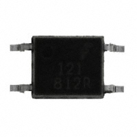
Marking Information
1
V X YY
3
4
121
2
R
6
5
Figure 20. Top Mark
Table 1. Top Mark Definitions
1
Fairchild Logo
2
Device Number
3
DIN EN/IEC60747-5-5 Option (only appears on component ordered with this option)
4
One-Digit Year Code, e.g., “5”
5
Digit Work Week, Ranging from “01” to “53”
6
Assembly Package Code
©2006 Fairchild Semiconductor Corporation
FODM121 Series, FODM124, FODM2701, FODM2705 Rev. 1.7
www.fairchildsemi.com
9
FODM121 Series, FODM124, FODM2701, FODM2705 — 4-Pin Full Pitch Mini-Flat Package Phototransistor Optocouplers
Ordering Information
�K0
P2
P0
t
D0
E
A0
W1
W
B0
d
F
D1
P
2.54 Pitch
Description
Symbol
Dimensions
Tape Width
W
12.00±0.4
Tape Thickness
t
0.35±0.02
Sprocket Hole Pitch
P0
4.00±0.20
Sprocket Hole Dia.
D0
1.55±0.20
Sprocket Hole Location
E
1.75±0.20
Pocket Location
F
5.50±0.20
P2
2.00±0.20
Pocket Pitch
P
8.00±0.20
Pocket Dimension
A0
4.75±0.20
B0
7.30±0.20
Pocket Hole Dia.
K0
2.30±0.20
D1
1.55±0.20
Cover Tape Width
W1
Cover Tape Thickness
d
Max. Component Rotation or Tilt
20° max
Devices Per Reel
2500
Reel Diameter
©2006 Fairchild Semiconductor Corporation
FODM121 Series, FODM124, FODM2701, FODM2705 Rev. 1.7
9.20
0.065±0.02
330 mm (13")
www.fairchildsemi.com
10
FODM121 Series, FODM124, FODM2701, FODM2705 — 4-Pin Full Pitch Mini-Flat Package Phototransistor Optocouplers
Carrier Tape Specifications
��ON Semiconductor and
are trademarks of Semiconductor Components Industries, LLC dba ON Semiconductor or its subsidiaries in the United States and/or other countries.
ON Semiconductor owns the rights to a number of patents, trademarks, copyrights, trade secrets, and other intellectual property. A listing of ON Semiconductor’s product/patent
coverage may be accessed at www.onsemi.com/site/pdf/Patent−Marking.pdf. ON Semiconductor reserves the right to make changes without further notice to any products herein.
ON Semiconductor makes no warranty, representation or guarantee regarding the suitability of its products for any particular purpose, nor does ON Semiconductor assume any liability
arising out of the application or use of any product or circuit, and specifically disclaims any and all liability, including without limitation special, consequential or incidental damages.
Buyer is responsible for its products and applications using ON Semiconductor products, including compliance with all laws, regulations and safety requirements or standards,
regardless of any support or applications information provided by ON Semiconductor. “Typical” parameters which may be provided in ON Semiconductor data sheets and/or
specifications can and do vary in different applications and actual performance may vary over time. All operating parameters, including “Typicals” must be validated for each customer
application by customer’s technical experts. ON Semiconductor does not convey any license under its patent rights nor the rights of others. ON Semiconductor products are not
designed, intended, or authorized for use as a critical component in life support systems or any FDA Class 3 medical devices or medical devices with a same or similar classification
in a foreign jurisdiction or any devices intended for implantation in the human body. Should Buyer purchase or use ON Semiconductor products for any such unintended or unauthorized
application, Buyer shall indemnify and hold ON Semiconductor and its officers, employees, subsidiaries, affiliates, and distributors harmless against all claims, costs, damages, and
expenses, and reasonable attorney fees arising out of, directly or indirectly, any claim of personal injury or death associated with such unintended or unauthorized use, even if such
claim alleges that ON Semiconductor was negligent regarding the design or manufacture of the part. ON Semiconductor is an Equal Opportunity/Affirmative Action Employer. This
literature is subject to all applicable copyright laws and is not for resale in any manner.
PUBLICATION ORDERING INFORMATION
LITERATURE FULFILLMENT:
Literature Distribution Center for ON Semiconductor
19521 E. 32nd Pkwy, Aurora, Colorado 80011 USA
Phone: 303−675−2175 or 800−344−3860 Toll Free USA/Canada
Fax: 303−675−2176 or 800−344−3867 Toll Free USA/Canada
Email: orderlit@onsemi.com
© Semiconductor Components Industries, LLC
N. American Technical Support: 800−282−9855 Toll Free
USA/Canada
Europe, Middle East and Africa Technical Support:
Phone: 421 33 790 2910
Japan Customer Focus Center
Phone: 81−3−5817−1050
www.onsemi.com
1
ON Semiconductor Website: www.onsemi.com
Order Literature: http://www.onsemi.com/orderlit
For additional information, please contact your local
Sales Representative
www.onsemi.com
�