Is Now Part of
To learn more about ON Semiconductor, please visit our website at
www.onsemi.com
Please note: As part of the Fairchild Semiconductor integration, some of the Fairchild orderable part numbers
will need to change in order to meet ON Semiconductor’s system requirements. Since the ON Semiconductor
product management systems do not have the ability to manage part nomenclature that utilizes an underscore
(_), the underscore (_) in the Fairchild part numbers will be changed to a dash (-). This document may contain
device numbers with an underscore (_). Please check the ON Semiconductor website to verify the updated
device numbers. The most current and up-to-date ordering information can be found at www.onsemi.com. Please
email any questions regarding the system integration to Fairchild_questions@onsemi.com.
ON Semiconductor and the ON Semiconductor logo are trademarks of Semiconductor Components Industries, LLC dba ON Semiconductor or its subsidiaries in the United States and/or other countries. ON Semiconductor owns the rights to a number
of patents, trademarks, copyrights, trade secrets, and other intellectual property. A listing of ON Semiconductor’s product/patent coverage may be accessed at www.onsemi.com/site/pdf/Patent-Marking.pdf. ON Semiconductor reserves the right
to make changes without further notice to any products herein. ON Semiconductor makes no warranty, representation or guarantee regarding the suitability of its products for any particular purpose, nor does ON Semiconductor assume any liability
arising out of the application or use of any product or circuit, and specifically disclaims any and all liability, including without limitation special, consequential or incidental damages. Buyer is responsible for its products and applications using ON
Semiconductor products, including compliance with all laws, regulations and safety requirements or standards, regardless of any support or applications information provided by ON Semiconductor. “Typical” parameters which may be provided in ON
Semiconductor data sheets and/or specifications can and do vary in different applications and actual performance may vary over time. All operating parameters, including “Typicals” must be validated for each customer application by customer’s
technical experts. ON Semiconductor does not convey any license under its patent rights nor the rights of others. ON Semiconductor products are not designed, intended, or authorized for use as a critical component in life support systems or any FDA
Class 3 medical devices or medical devices with a same or similar classification in a foreign jurisdiction or any devices intended for implantation in the human body. Should Buyer purchase or use ON Semiconductor products for any such unintended
or unauthorized application, Buyer shall indemnify and hold ON Semiconductor and its officers, employees, subsidiaries, affiliates, and distributors harmless against all claims, costs, damages, and expenses, and reasonable attorney fees arising out
of, directly or indirectly, any claim of personal injury or death associated with such unintended or unauthorized use, even if such claim alleges that ON Semiconductor was negligent regarding the design or manufacture of the part. ON Semiconductor
is an Equal Opportunity/Affirmative Action Employer. This literature is subject to all applicable copyright laws and is not for resale in any manner.
�FPDB30PH60
PFC SPM® 3 Series for 2-Phase Bridgeless PFC
Features
General Description
The FPDB30PH60 is a PFC SPM® 3 module providing a
fully-featured, high-performance Bridgeless PFC (Power
Factor Correction) input power stage for consumer,
medical, and industrial applications. These modules
integrate optimized gate drive of the built-in IGBTs to
minimize
EMI
and
losses,
while
also
providing multiple on-module
protection
features
including under-voltage lockout, over-current shutdown,
thermal monitoring, and fault reporting. These modules
also feature high-performance output diodes and shunt
resistor for additional space savings and mounting
convenience.
• UL Certified No. E209204 (UL1557)
• 600 V - 30 A 2-Phase Bridgeless PFC with Integral
Gate Driver and Protection
• Very Low Thermal Resistance Using
Substrate
Al2O3 DBC
• Built-in NTC Thermistor for Temperature Monitoring
• Built-in Shunt Resistor for Current Sensing
• Optimized for 20kHz Switching Frequency
• Isolation Rating: 2500 Vrms/min.
Applications
• 2-Phase Bridgeless PFC Converter
Related Source
• AN-9041 - Bridgeless PFC SPM 3 Series Design
Guide
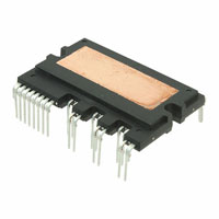
Figure 1. Package Overview
Package Marking & Ordering Information
Device
Device Marking
Package
Packing Type
Quantity
FPDB30PH60
FPDB30PH60
SPMGA-027
Rail
10
©2005 Fairchild Semiconductor Corporation
FPDB30PH60 Rev. C3
1
www.fairchildsemi.com
FPDB30PH60 PFC SPM® 3 Series for 2-Phase Bridgeless PFC
December 2013
�• PFC converter for single-phase AC / DC power conversion.(please refer to Figure 3)
Integrated Drive, Protection and System Control Functions
• For IGBTs: gate drive circuit, Over-Current Protection (OCP), control supply circuit Under-Voltage Lock-Out (UVLO) Protection
• Fault signal: corresponding to OC and UV fault
• Built-in thermistor: temperature monitoring
• Input interface: active-HIGH interface, works with 3.3 / 5 V logic, Schmitt-trigger input
Pin Configuration
(1) VCC(L)
(2) COM
(3) NC
(4) IN(R)
(5) IN(S)
(6) VFO
(7) CFOD
(8) CSC
(21) VAC(22) NSENSE
(23) NC
N
(9) NC
(10) NC
(11) NC
(12) NC
(13) NC
(14) NC
(15) NC
(24) N
Case Temperature (T C)
Detecting Point
(25) R
(16) NC
(17) NC
(18) NC
(26) S
DBC Substrate
(19) RTH
(27) PR
(20) VTH
Figure 2. Top View
©2005 Fairchild Semiconductor Corporation
FPDB30PH60 Rev. C3
2
www.fairchildsemi.com
FPDB30PH60 PFC SPM® 3 Series for 2-Phase Bridgeless PFC
Integrated Power Functions
�FPDB30PH60 PFC SPM® 3 Series for 2-Phase Bridgeless PFC
Pin Descriptions
Pin Number
Pin Name
Pin Description
1
VCC
Common Bias Voltage for IC and IGBTs Driving
2
COM
Common Supply Ground
4
IN(R)
Signal Input for Low-Side R-Phase IGBT
5
IN(S)
Signal Input for Low-Side S-Phase IGBT
6
VFO
Fault Output
7
CFOD
Capacitor for Fault Output Duration Selection
8
CSC
Capacitor(Low-Pass Filter) for Over-Current Detection
19
R(TH)
Series Resistor for The Use of Thermistor
20
V(TH)
Thermistor Bias Voltage
21
VAC-
Current Sensing Terminal
22
NSENSE
24
N
Negative Rail of DC-Link
25
R
Output for R-Phase
26
S
Output for S-Phase
27
PR
Positive Rail of DC-Link
3, 9~18, 23
NC
No Connection
Current Sensing Reference Terminal
Internal Equivalent Circuit
(20) V TH
(19) R TH
NTC
Thermistor
(27) P R
D1
D2
(8) C SC
CSC
(26) S
(7) C FOD
CFOD
(25) R
(6) V FO
VFO
(5) IN (S)
IN(S)
(4) IN (R)
IN(R)
OUT(S)
Q1
D3
Q2
D4
(24) N
(23) NC
OUT(R)
(2) COM
COM
(1) VCC
VCC
Shunt
Resistor
(22) N SENSE
(21) V AC-
Figure 3. Internal Block Diagram
Notes:
1. Converter is composed of two IGBTs including four diodes and one IC which has gate driving and protection functions.
©2005 Fairchild Semiconductor Corporation
FPDB30PH60 Rev. C3
3
www.fairchildsemi.com
�unless otherwise specified.)
Converter Part
Symbol
Item
Vi
Vi(Surge)
VPN
VPN(Surge)
Condition
Rating
Unit
Supply Voltage
Applied between R - S
264
Vrms
Supply Voltage (Surge)
Applied between R - S
500
V
Output Voltage
Applied between P - N
450
V
Output Voltage (Surge)
Applied between P - N
500
V
600
V
VCES
Collector - Emitter Voltage
Ii
Input Current (100% Load)
TC < 95°C, Vi = 220 V, VPN = 390 V,
VPWM = 20 kHz
20
A
Ii(125%)
Input Current (125% Load)
TC < 95°C, Vi = 220V , VPN = 390 V,
VPWM = 20 kHz, 1 min Non-Repetitive
25
A
Collector Dissipation
TC = 25°C per IGBT
83
W
PRSH
Power Rating of Shunt Resistor
TC < 125°C
2
W
TJ
Operating Junction Temperature
(Note 2)
-20 ~ 125
°C
PC
Notes:
2. The maximum junction temperature rating of the power chips integrated within the PFC SPM® product is 150 C(@TC 100C). However, to insure safe operation of the PFC
SPM product, the average junction temperature should be limited to TJ(ave) 125C (@TC 100C)
Control Part
Symbol
Item
Condition
VCC
Control Supply Voltage
Applied between VCC - COM
VIN
Input Signal Voltage
Applied between IN - COM
VFO
Fault Output Supply Voltage
Applied between VFO - COM
IFO
Fault Output Current
Sink Current at VFO Pin
VSC
Current Sensing Input Voltage
Applied between CSC - COM
Rating
Unit
20
V
-0.3 ~ 17.0
V
-0.3 ~ VCC+0.3
V
5
mA
-0.3~VCC+0.3
V
Total System
Symbol
Rating
Unit
Module Case Operation Temperature
-20 ~ 100
°C
TSTG
Storage Temperature
-40 ~ 125
°C
VISO
Isolation Voltage
2500
Vrms
TC
Item
Condition
60 Hz, Sinusoidal, AC 1 Minute, Connect
Pins to Heat-Sink Plate
Thermal Resistance
Symbol
R(j-c)Q
R(j-c)HD
Item
Junction to Case Thermal Resistance
(Referenced to PKG Center)
R(j-c)LD
Condition
Min.
Typ.
Max.
Unit
IGBT
-
-
1.2
°C/W
High-Side Diode
-
-
2.0
°C/W
Low-Side Diode
-
-
1.4
°C/W
Notes :
3. For the measurement point of case temperature(TC), please refer to Figure 2.
©2005 Fairchild Semiconductor Corporation
FPDB30PH60 Rev. C3
4
www.fairchildsemi.com
FPDB30PH60 PFC SPM® 3 Series for 2-Phase Bridgeless PFC
Absolute Maximum Ratings (TJ = 25°C,
�Converter Part
Symbol
Item
Condition
Min.
Typ.
Max. Unit
VCE(SAT)
IGBT Saturation Voltage
VCC = 15 V, VIN = 5 V, IC =30 A
-
2.4
3.1
V
VFH
High-Side Diode Voltage
IF = 30 A
-
1.9
2.5
V
VFL
Low-Side Diode Voltage
IF = 30 A
-
1.2
1.6
V
tON
Switching Times
VPN = 400 V, VCC = 15 V, IC =30 A
VIN = 0 V 5 V, Inductive Load
-
550
-
ns
-
200
-
ns
-
430
-
ns
tC(OFF)
-
180
-
ns
trr
-
60
-
ns
Irr
-
6
-
A
1.8
2.0
2.2
m
-
-
250
A
tC(ON)
(Note 4)
tOFF
RSENSE
Current-Sensing Resistor
ICES
Collector - Emitter
Leakage Current
VCE = VCES
Notes:
4. tON and tOFF include the propagation delay of the internal drive IC. tC(ON) and tC(OFF) are the switching time of IGBT itself under the given gate driving condition internally. For
the detailed information, please see Figure 4.
Irr
120% of IC
100% of IC
VCE
IC
90% of IC
10% of VCE
IC
10% of IC
VCE 10% of VCE
10% of IC
VIN
VIN
tON
trr
tC(OFF)
tC(ON)
tOFF
(a) Turn-on
(b) Turn-off
Figure 4. Switching Time Definition
©2005 Fairchild Semiconductor Corporation
FPDB30PH60 Rev. C3
5
www.fairchildsemi.com
FPDB30PH60 PFC SPM® 3 Series for 2-Phase Bridgeless PFC
Electrical Characteristics (TJ = 25°C, unless otherwise specified.)
�Symbol
Item
Condition
IQCCL
Quiescent VCC Supply Current
VCC = 15 V, IN = 0 V VCC - COM
VFOH
Fault Output Voltage
VFOL
Min.
Typ.
Max. Unit
-
-
26
mA
VSC = 0 V, VFO Circuit: 4.7 k to 5 V Pull-up
4.5
-
-
V
VSC = 1 V, VFO Circuit: 4.7 k to 5 V Pull-up
-
-
0.8
V
VSC(ref)
Over-Current Trip Level
VCC = 15 V
0.45
0.50
0.55
V
UVCCD
Supply Circuit Under-Voltage
Protection
Detection Level
10.7
11.9
13.0
V
Reset Level
11.2
12.4
13.2
V
UVCCR
tFOD
Fault-Out Pulse Width
CFOD = 33 nF (Note 5)
1.4
1.8
2.0
ms
VIN(ON)
ON Threshold Voltage
Applied between IN - COM
3.0
-
-
V
VIN(OFF)
OFF Threshold Voltage
-
-
0.8
V
at TC = 25°C (See Figure 5)
-
50
-
k
at TC = 80°C (See Figure 5)
-
5.76
-
k
RTH
Resistance of Thermistor
Notes:
5. The fault-out pulse width tFOD depends on the capacitance value of CFOD according to the following approximate equation : CFOD = 18.3 x 10⁻⁶ x tFOD[F]
R-T Graph
120
Resistance [k]
100
80
60
40
20
0
20
30
40
50
60
70
80
90 100 110 120 130
Temperature [C]
Figure 5. R-T Curve of the Built-in Thermistor
Recommended Operating conditions
Symbol
VI
Item
Condition
Min.
Typ.
Max.
Unit
Input Supply Voltage
Applied between R - S
180
-
264
Vrms
VPN
Output Voltage
Applied between P - N
-
280
400
V
VCC
Control Supply Voltage
Applied between VCC - COM
13.5
15.0
16.5
V
dVCC/dt
Control Supply Variation
Applied between IN - COM
-1
-
1
V/s
PWM Input Signal
TC 100°C, TJ 125°C, per IGBT
-
20
-
kHz
fPWM
©2005 Fairchild Semiconductor Corporation
FPDB30PH60 Rev. C3
6
www.fairchildsemi.com
FPDB30PH60 PFC SPM® 3 Series for 2-Phase Bridgeless PFC
Control Part
�Item
Condition
Mounting Torque
Mounting Screw: M3
Device Flatness
See Figure 6
Recommended 0.62 N•m
Weight
Min.
Typ.
Max.
Units
0.51
0.62
0.72
N•m
0
-
+120
m
-
15.00
-
g
(+)
(+)
(+)
Figure 6. Flatness Measurement Position
©2005 Fairchild Semiconductor Corporation
FPDB30PH60 Rev. C3
7
www.fairchildsemi.com
FPDB30PH60 PFC SPM® 3 Series for 2-Phase Bridgeless PFC
Mechanical Characteristics and Ratings
�FPDB30PH60 PFC SPM® 3 Series for 2-Phase Bridgeless PFC
Time Charts of Protective Function
In p u t S ig n a l
In te rn a l IG B T
G a te -E m itte r V o lta g e
P3
UV
re se t
P5
C o n tro l S u p p ly V o lta g e
P2
UV
d e te c t
P6
P1
O u tp u t C u rre n t
P4
F a u lt O u tp u t S ig n a l
P1 : Normal operation: IGBT ON and conducting current.
P2 : Under-voltage detection.
P3 : IGBT gate interrupt.
P4 : Fault signal generation.
P5 : Under-voltage reset.
P6 : Normal operation: IGBT ON and conducting current.
Figure 7. Under-Voltage Protection
P5
In p u t S ig n a l
P6
In te rn a l IG B T
G a te -E m itte r V o lta g e
O C D e te c tio n
P1
P4
P7
O u tp u t C u rre n t
P2
O C R e fe re n c e
V o lta g e (0 .5 V )
S e n s in g V o lta g e
R C F ilte r D e la y
F a u lt O u tp u t S ig n a l
P3
P8
P1 : Normal operation: IGBT ON and conducting current.
P2 : Over current detection.
P3 : IGBT gate interrupt / fault signal generation.
P4 : IGBT is slowly turned off.
P5 : IGBT OFF signal.
P6 : IGBT ON signal: but IGBT cannot be turned on during the fault output activation.
P7 : IGBT OFF state.
P8 : Fault output reset and normal operation start.
Figure 8. Over-Current Protection
©2005 Fairchild Semiconductor Corporation
FPDB30PH60 Rev. C3
8
www.fairchildsemi.com
�+5 V
VTH
RTH
CSC
MCU
CFOD
VFO
or
Controller
IN(S)
IN(R)
NTC
Thermistor
PR
S
CSC
R
CFOD
3-Phase
Inverter
VFO
IN(S)
OUT(S)
IN(R)
COM
COM
N
OUT(R)
Shunt
Resistor
VCC
NSENSE
VAC-
VCC
Figure 9. Application Example
Notes:
6. For the over-current protection, please set time constant in the range 3 ~ 4 s.
©2005 Fairchild Semiconductor Corporation
FPDB30PH60 Rev. C3
9
www.fairchildsemi.com
FPDB30PH60 PFC SPM® 3 Series for 2-Phase Bridgeless PFC
Vac
�FPDB30PH60 PFC SPM® 3 Series for 2-Phase Bridgeless PFC
Detailed Package Outline Drawings
Package drawings are provided as a service to customers considering Fairchild components. Drawings may change in any manner
without notice. Please note the revision and/or data on the drawing and contact a FairchildSemiconductor representative to verify or
obtain the most recent revision. Package specifications do not expand the terms of Fairchild’s worldwide therm and conditions,
specifically the the warranty therein, which covers Fairchild products.
Always visit Fairchild Semiconductor’s online packaging area for the most recent package drawings:
http://www.fairchildsemi.com/dwg/MO/MOD27BA.pdf
©2005 Fairchild Semiconductor Corporation
FPDB30PH60 Rev. C3
10
www.fairchildsemi.com
�FPDB30PH60 PFC SPM® 3 Series for 2-Phase Bridgeless PFC
©2005 Fairchild Semiconductor Corporation
FPDB30PH60 Rev. C3
11
www.fairchildsemi.com
�ON Semiconductor and
are trademarks of Semiconductor Components Industries, LLC dba ON Semiconductor or its subsidiaries in the United States and/or other countries.
ON Semiconductor owns the rights to a number of patents, trademarks, copyrights, trade secrets, and other intellectual property. A listing of ON Semiconductor’s product/patent
coverage may be accessed at www.onsemi.com/site/pdf/Patent−Marking.pdf. ON Semiconductor reserves the right to make changes without further notice to any products herein.
ON Semiconductor makes no warranty, representation or guarantee regarding the suitability of its products for any particular purpose, nor does ON Semiconductor assume any liability
arising out of the application or use of any product or circuit, and specifically disclaims any and all liability, including without limitation special, consequential or incidental damages.
Buyer is responsible for its products and applications using ON Semiconductor products, including compliance with all laws, regulations and safety requirements or standards,
regardless of any support or applications information provided by ON Semiconductor. “Typical” parameters which may be provided in ON Semiconductor data sheets and/or
specifications can and do vary in different applications and actual performance may vary over time. All operating parameters, including “Typicals” must be validated for each customer
application by customer’s technical experts. ON Semiconductor does not convey any license under its patent rights nor the rights of others. ON Semiconductor products are not
designed, intended, or authorized for use as a critical component in life support systems or any FDA Class 3 medical devices or medical devices with a same or similar classification
in a foreign jurisdiction or any devices intended for implantation in the human body. Should Buyer purchase or use ON Semiconductor products for any such unintended or unauthorized
application, Buyer shall indemnify and hold ON Semiconductor and its officers, employees, subsidiaries, affiliates, and distributors harmless against all claims, costs, damages, and
expenses, and reasonable attorney fees arising out of, directly or indirectly, any claim of personal injury or death associated with such unintended or unauthorized use, even if such
claim alleges that ON Semiconductor was negligent regarding the design or manufacture of the part. ON Semiconductor is an Equal Opportunity/Affirmative Action Employer. This
literature is subject to all applicable copyright laws and is not for resale in any manner.
PUBLICATION ORDERING INFORMATION
LITERATURE FULFILLMENT:
Literature Distribution Center for ON Semiconductor
19521 E. 32nd Pkwy, Aurora, Colorado 80011 USA
Phone: 303−675−2175 or 800−344−3860 Toll Free USA/Canada
Fax: 303−675−2176 or 800−344−3867 Toll Free USA/Canada
Email: orderlit@onsemi.com
© Semiconductor Components Industries, LLC
N. American Technical Support: 800−282−9855 Toll Free
USA/Canada
Europe, Middle East and Africa Technical Support:
Phone: 421 33 790 2910
Japan Customer Focus Center
Phone: 81−3−5817−1050
www.onsemi.com
1
ON Semiconductor Website: www.onsemi.com
Order Literature: http://www.onsemi.com/orderlit
For additional information, please contact your local
Sales Representative
www.onsemi.com
�