Is Now Part of
To learn more about ON Semiconductor, please visit our website at
www.onsemi.com
Please note: As part of the Fairchild Semiconductor integration, some of the Fairchild orderable part numbers
will need to change in order to meet ON Semiconductor’s system requirements. Since the ON Semiconductor
product management systems do not have the ability to manage part nomenclature that utilizes an underscore
(_), the underscore (_) in the Fairchild part numbers will be changed to a dash (-). This document may contain
device numbers with an underscore (_). Please check the ON Semiconductor website to verify the updated
device numbers. The most current and up-to-date ordering information can be found at www.onsemi.com. Please
email any questions regarding the system integration to Fairchild_questions@onsemi.com.
ON Semiconductor and the ON Semiconductor logo are trademarks of Semiconductor Components Industries, LLC dba ON Semiconductor or its subsidiaries in the United States and/or other countries. ON Semiconductor owns the rights to a number
of patents, trademarks, copyrights, trade secrets, and other intellectual property. A listing of ON Semiconductor’s product/patent coverage may be accessed at www.onsemi.com/site/pdf/Patent-Marking.pdf. ON Semiconductor reserves the right
to make changes without further notice to any products herein. ON Semiconductor makes no warranty, representation or guarantee regarding the suitability of its products for any particular purpose, nor does ON Semiconductor assume any liability
arising out of the application or use of any product or circuit, and specifically disclaims any and all liability, including without limitation special, consequential or incidental damages. Buyer is responsible for its products and applications using ON
Semiconductor products, including compliance with all laws, regulations and safety requirements or standards, regardless of any support or applications information provided by ON Semiconductor. “Typical” parameters which may be provided in ON
Semiconductor data sheets and/or specifications can and do vary in different applications and actual performance may vary over time. All operating parameters, including “Typicals” must be validated for each customer application by customer’s
technical experts. ON Semiconductor does not convey any license under its patent rights nor the rights of others. ON Semiconductor products are not designed, intended, or authorized for use as a critical component in life support systems or any FDA
Class 3 medical devices or medical devices with a same or similar classification in a foreign jurisdiction or any devices intended for implantation in the human body. Should Buyer purchase or use ON Semiconductor products for any such unintended
or unauthorized application, Buyer shall indemnify and hold ON Semiconductor and its officers, employees, subsidiaries, affiliates, and distributors harmless against all claims, costs, damages, and expenses, and reasonable attorney fees arising out
of, directly or indirectly, any claim of personal injury or death associated with such unintended or unauthorized use, even if such claim alleges that ON Semiconductor was negligent regarding the design or manufacture of the part. ON Semiconductor
is an Equal Opportunity/Affirmative Action Employer. This literature is subject to all applicable copyright laws and is not for resale in any manner.
�FPF1015/6/7/8
IntelliMAX
TM
tm
1V Rated Advanced Load Management Products
Features
General Description
0.8 to 1.8V Input Voltage Range
The FPF1015/6/7/8 series is an IntelliMAX advanced slew rate
loadswitch offering a very low operating voltage. These devices
consist of a 34mΩ N-channel MOSFET that supports an input
voltage up to 2.0V. These slew rate devices control the switch
turn-on and prevent excessive in-rush current from the supply
rails. The input voltage range operates from 0.8V to 1.8V to
fulfill today's lowest Ultraportable Device's supply requirements.
Switch control is via a logic input (ON) capable of interfacing
directly with low voltage control signals.
Typical RDS(ON) = 34mΩ @ VON - VIN = 2.0V
Output Discharge Function
Internal Pull down at ON Pin
Accurate Slew Rate Controlled Turn-on time
Low < 1µA Quiescent Current
ESD Protected, above 8000V HBM, 2000V CDM
RoHS Compliant
The FPF1016 and FPF1018 have an On-Chip pull down
allowing for quick and controlled output discharge when switch
is turned off. The FPF1015/6/7/8 series is available in a
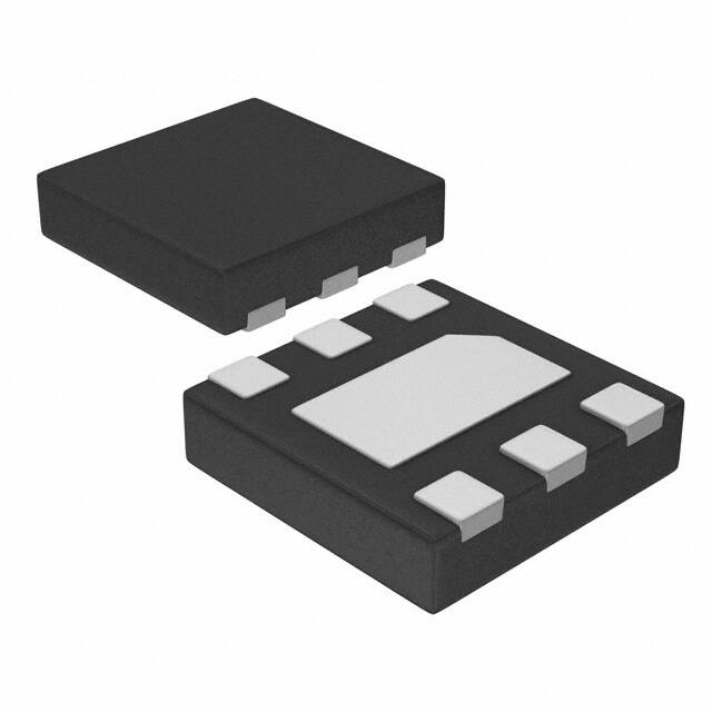
space-saving 2X2 MLP-6L package.
Free from Halogenated Compounds and Antimony Oxides
Applications
PDAs
Cell Phones
GPS Devices
MP3 Players
Digital Cameras
Notebook Computers
PIN 1
TOP
BOTTOM
Typical Application Circuit
TO LOAD
VOUT
VIN
FPF1015/6/7/8
OFF ON
ON
-
COUT
GND
CIN
Ordering Information
Part
Switch
Turn-on Time
Output Discharge
ON Pin Activity
Package
FPF1015
34mΩ, NMOS
43us
NA
Active HI
MLP 2x2
FPF1016
34mΩ, NMOS
43us
60Ω
Active HI
MLP 2x2
FPF1017
34mΩ, NMOS
165us
NA
Active HI
MLP 2x2
FPF1018
34mΩ, NMOS
165us
60Ω
Active HI
MLP 2x2
©2009 Fairchild Semiconductor Corporation
FPF1015/6/7/8 Rev. D
1
www.fairchildsemi.com
FPF1015/6/7/8 IntelliMAXTM 1V Rated Advanced Load Management Products
June 2009
�FPF1015/6/7/8 IntelliMAXTM 1V Rated Advanced Load Management Products
Functional Block Diagram
VIN
CONTROL
LOGIC
ON
Turn-on Slew Rate
Controlled Driver
VOUT
ESD protection
Output Discharge
(Optional for FPF1016/18)
FPF1015/6/7/8
GND
Pin Configuration
GND 6
1 ON
VOUT 5
2 VIN
VOUT 4
3 VIN
MicroFET 2x2 6L BOTTOM VIEW
Pin Description
Pin
Name
1
ON
ON/OFF Control Input, 2nd Supply
Function
Supply Input: Input to the power switch
2, 3
VIN
4, 5
VOUT
Switch Output.
6
GND
Ground
Absolute Maximum Ratings
Parameter
Min
Max
Unit
VIN, VOUT to GND
-0.3
2
V
VON to GND
-0.3
4.2
V
1.5
A
Maximum Continuous Switch Current
1.2
W
Operating Temperature Range
Power Dissipation @ TA = 25°C (Note 1)
-40
85
°C
Storage Temperature
-65
150
°C
86
°C/W
Thermal Resistance, Junction to Ambient
Electrostatic Discharge Protection
HBM
8000
V
CDM
2000
V
Recommended Operating Range
Parameter
Min
Max
Unit
VIN
0.8
1.8
V
Ambient Operating Temperature, TA
-40
85
°C
Note 1: Package power dissipation on 1square inch pad, 2 oz. copper board
FPF1015/6/7/8 Rev. D
2
www.fairchildsemi.com
�VIN = 0.8 to 1.8V, TA = -40 to +85°C unless otherwise noted. Typical values are at VIN = 1.8V and TA = 25°C.
Parameter
Symbol
Conditions
Min
Typ
Max
Unit
1.8
V
1.8
2.8
4.0
V
2.8
3.8
Basic Operation
Operating Voltage
ON input Voltage
0.8
VIN
VON(MIN)
VIN = 0.8V
4.0
V
ICC
VIN = 1V, VON = 3.3V, VOUT = Open
1
µA
Quiescent Current
IQ
VIN = 1V, VON = VOUT = Open
2
µA
Off Switch Current
ISWOFF
VIN = 1.8V, VON = GND, VOUT = GND
2
µA
Operating Current
VON(MAX) VIN = 1.8V(Note2)
On-Resistance
RON
Output Pull Down Resistance
RPD
ON Input Logic Low Voltage
VIL
VIN = 1V, VON = 3V, ILOAD = 1A, TA = 25°C
34
45
VIN = 1V, VON = 2.3V, ILOAD = 1A, TA = 25°C
41
55
VIN = 1V, VON = 0V, TA = 25°C, ILOAD = 1mA,
FPF1016, FPF1018
60
120
VIN = 0.8V, RLOAD = 1KΩ
0.3
VIN = 1.8V, RLOAD = 1KΩ
0.8
VON = VIN or GND
ON Input Leakage
-1
1
mΩ
Ω
V
µA
Dynamic (VIN = 1.0V, VON = 3.0V, TA = 25°C)
VOUT Rise Time
Turn ON
VOUT Fall Time
Turn Off
TR
TON
TF
TOFF
FPF1015, FPF1016, RL = 500Ω, CL = 0.1µF
28
FPF1017, FPF1018, RL = 500Ω, CL = 0.1µF
114
FPF1015, FPF1016, RL = 3.3Ω, CL = 10µF
38
FPF1017, FPF1018, RL = 3.3Ω, CL = 10µF
155
FPF1015, FPF1016, RL = 500Ω, CL = 0.1µF
43
FPF1017, FPF1018, RL = 500Ω, CL = 0.1µF
165
FPF1015, FPF1016, RL = 3.3Ω, CL = 10µF
58
FPF1017, FPF1018, RL = 3.3Ω, CL = 10µF
228
FPF1015, FPF1017, RL = 500Ω, CL = 0.1µF
105
FPF1016, FPF1018,
RPD = 60Ω, RL = 500Ω, CL = 0.1µF
15
FPF1015, FPF1017, RL = 3.3Ω, CL = 10µF
80
FPF1016, FPF1018
RPD = 60Ω, RL = 3.3Ω, CL = 10µF
74
FPF1015, FPF1017, RL = 500Ω, CL = 0.1µF
150
FPF1016, FPF1018
RPD = 60Ω, RL = 500Ω, CL = 0.1µF
53
FPF1015, FPF1017, RL = 3.3Ω, CL = 10µF
102
FPF1016, FPF1018
RPD = 60Ω, RL = 3.3Ω, CL = 10µF
96
µs
µs
µs
µs
Note 2: VON(MAX) is limited by the absolute rating.
FPF1015/6/7/8 Rev. D
3
www.fairchildsemi.com
FPF1015/6/7/8 IntelliMAXTM 1V Rated Advanced Load Management Products
Electrical Characteristics
�12
0.02
0.018
VON = 0V
10
0.014
VON = 0V
VOUT = Open
VIN = 1.8V
VIN = 1.0V
8
0.012
IQ (uA)
Supply Current (uA)
0.016
0.01
0.008
4
VON =3.3V
0.006
6
0.004
2
0.002
VIN = 0.8V
0
0.8
1
1.2
1.4
1.6
0
-50
1.8
-25
0
Figure 1. Supply Current vs.VIN
9
VIN = 1.8V
8
ISWOFF ( uA)
0.12
0.1
ICC (uA)
75
100
125
100
125
10
VON = 3.3V
VOUT = Open
0.14
0.08
VIN = 1.0V
0.06
0.04
VIN = 1.8V
VON = 0V
VOUT = 0V
7
6
5
4
3
2
0.02
1
VIN = 0.8V
0
-50
-25
0
25
50
75
100
0
-50
125
TJ, Junction Temperature (oC)
-25
0
25
50
75
TJ, Junction Temperature oC
Figure 3. Operating Current vs. Temperature
Figure 4. Off Switch Current vs. Temperature
45
60
VIN = 1 V
VON = 3 V
IOUT = 1 A
VON = 3V
IOUT = 1A
55
On Resistance (mOhms)
On Resistance (mOhms)
50
Figure 2. Quiescent Current vs. Temperature
0.16
40
25
TJ, Junction Temperature oC
Supply Voltage (V)
35
30
25
50
45
40
35
30
25
20
-50
-25
0
25
50
75
100
20
1.2 1.3 1.4 1.5 1.6 1.7 1.8 1.9
125
TJ, Junction Temperature (oC)
Figure 5. RON vs. Temperature
FPF1015/6/7/8 Rev. D
2
2.1 2.2 2.3 2.4 2.5 2.6 2.7
VON - VIN (V)
Figure 6. RON vs. VON - VIN
4
www.fairchildsemi.com
FPF1015/6/7/8 IntelliMAXTM 1V Rated Advanced Load Management Products
Typical Characteristics
�1.5
1.4
VIN = 1.8V
On Threshold Voltage, VIL (V)
On Threshold Voltage (V)
1.2
1
0.8
0.6
0.4
0.2
0
0.8
0.9
1
1.1
1.2
1.3
1.4
1.5
1.6
1.7
1.2
0.9
VIN = 1.0V
0.6
VIN = 0.8V
0.3
0
-50
1.8
-25
0
Figure 7. VIL vs. VIN
VIN = 1V
VON = 3V
RL = 3.3 Ohm
CL = 10uF
250
Turn ON/OFF Time (us)
Rise/Fall Time (us)
75
100
125
300
FPF1017 / 18 TRISE
100
50
Figure 8. VIL vs. Temperature
200
150
25
TJ, Junction Temperature (oC)
Supply Voltage (V)
FPF1016 / 18 TFALL
50
-15
10
35
150
FPF1016 / 18 TOFF
100
50
FPF1015 / 16 TRISE
0
-40
200
FPF1017 / 18 TON
VIN = 1V
VON = 3V
RL = 3.3 Ohm
CL = 10uF
60
FPF1015 / 16 TON
0
-40
85
-15
TJ, Junction temperature (oC)
Figure 9. TRISE/TFALL vs. Temperature
VON
2V/DIV
IOUT
500mA/DIV
IOUT
500mA/DIV
VOUT
500mV/DIV
VIN = 1V
VON = 2.6V
CIN = 10uF
CL= 10uF
RL = 3.3Ω
VIN
500mV/DIV
VOUT
500mV/DIV
100us/DIV
60
85
VIN = 1V
VON = 2.6V
CIN = 10uF
CL = 4.7uF
RL = 1Ω
100us/DIV
Figure 11. FPF1015 / 16 Turn ON response
FPF1015/6/7/8 Rev. D
35
Figure 10. TON/TOFF vs. Temperature
VON
2V/DIV
VIN
500mV/DIV
10
TJ, Junction Temperature (oC)
Figure 12. FPF1015 / 16 Turn ON response
5
www.fairchildsemi.com
FPF1015/6/7/8 IntelliMAXTM 1V Rated Advanced Load Management Products
Typical Characteristics
�VON
2V/DIV
VON
2V/DIV
IOUT
500mA/DIV
IOUT
500mA/DIV
VIN
500mV/DIV
VOUT
500mV/DIV
VIN = 1V
VON = 2.6V
CIN = 10uF
CL = 10uF
RL = 3.3Ω
VIN
500mV/DIV
VOUT
500mV/DIV
100us/DIV
100us/DIV
Figure 13. FPF1017 / 18 Turn On response
Figure 14. FPF1017 / 18 Turn On response
VON
2V/DIV
VON
2V/DIV
IOUT
500mA/DIV
IOUT
500mA/DIV
VIN = 1V
VON = 2.6V
CIN = 10uF
CL= 10uF
RL = 3.3Ω
IVIN
500mV/DIV
VOUT
500mV/DIV
VIN
500mV/DIV
VOUT
500mV/DIV
100us/DIV
Figure 16. FPF105 / 17 Turn OFF response
VON
2V/DIV
VON
2V/DIV
IOUT
500mA/DIV
IOUT
500mA/DIV
VIN = 1V
VON = 2.6V
CIN = 10uF
CL = 10uF
RL = 3.3Ω
VOUT
500mV/DIV
VIN = 1V
VON = 2.6V
CIN = 10uF
CL = 4.7uF
RL = 1Ω
VIN
500mV/DIV
VOUT
500mV/DIV
100us/DIV
100us/DIV
Figure 17. FPF1016 / 18 Turn OFF response
FPF1015/6/7/8 Rev. D
VIN = 1V
VON = 2.6V
CIN = 10uF
CL = 47uF
RL = 1Ω
100us/DIV
Figure 15. FPF1015 / 17 Turn OFF response
VIN
500mV/DIV
VIN = 1V
VON = 2.6V
CIN = 10uF
CL = 47uF
RL = 1Ω
Figure 18. FPF1016 / 18 Turn OFF response
6
www.fairchildsemi.com
FPF1015/6/7/8 IntelliMAXTM 1V Rated Advanced Load Management Products
Typical Characteristics
�FPF1015/6/7/8 IntelliMAXTM 1V Rated Advanced Load Management Products
Typical Characteristics
VON
2V/DIV
VIN
500mV/DIV
VOUT
500mV/DIV
VIN = 1V
VON = 2.6V
CIN = 10uF
RL = 499Ω
20us/DIV
Figure 19. FPF1016 / 18 Output Pull Down response
FPF1015/6/7/8 Rev. D
7
www.fairchildsemi.com
�Timing Diagram
The FPF1015/6/7/8 are low RDS(ON) N-Channel load switches
with controlled turn-on. The core of each device is a 34mΩ
(VIN = 1V, VON = 3V) N-Channel MOSFET and is customized for
a low input operating range of 0.8 to 1.8V. The ON pin controls
the state of the switch.
90%
VON
The FPF1016 and FPF1018 contain a 60Ω(typ) on-chip resistor
which is connected internally from VOUT to GND for quick output
discharge when the switch is turned off.
10%
90%
90%
VOUT
10%
10%
tdON tR
On/Off Control
tdOFF tF
tON
The ON pin is active high and it controls the state of the switch.
Applying a continuous high signal will hold the switch in the ON
state. In order to minimize the switch on resistance, the ON pin
voltage should exceed the input voltage by 2V. This device is
compatible with a GPIO (General Purpose Input/Output) port,
where the logic voltage level can be configured to 4V ≥ VON ≥
VIN+2V and power consumed is less than 1µA in steady state.
where:
tdON
tR
tON
tdOFF
tF
tOFF
=
=
=
=
=
=
tOFF
Delay On Time
VOUT Rise Time
Turn On Time
Delay Off Time
VOUT Fall Time
Turn Off Time
Application Information
Typical Application
VOUT
VIN
VIN = 0.8-1.8V
FPF1015/6/7/8
CIN
OFF ON
RL
CL
ON
GND
Input Capacitor
Board Layout
To limit the voltage drop on the input supply caused by transient
in-rush currents when the switch turns-on, a capacitor must be
placed between VIN and GND. For minimized voltage drop,
especially when the operating voltage approaches 1V and a fast
slew rate part (FPF1015 and FPF1016) is selected, a 10µF
ceramic capacitor should be placed close to the VIN pins. Higher
values of CIN can be used to further reduce the voltage drop
during higher current modes of operation.
For best performance, all traces should be as short as possible.
To be most effective, the input and output capacitors should be
placed close to the device to minimize the effects that parasitic
trace inductances may have on normal and short-circuit
operation. Using wide traces or large copper planes for all pins
(VIN, VOUT, ON and GND) will help minimize the parasitic
electrical effects along with minimizing the case to ambient
thermal impedance.
Output Capacitor
A 0.1µF capacitor, CL, should be placed between VOUT and
GND. This capacitor will prevent parasitic board inductance
from forcing VOUT below GND when the switch turns-off. If the
application has a capacitive load, the FPF1016 and FPF1018
can be used to discharged that load through an on-chip output
discharge path.
FPF1015/6/7/8 Rev. D
8
www.fairchildsemi.com
FPF1015/6/7/8 IntelliMAXTM 1V Rated Advanced Load Management Products
Description of Operation
�Demo Board Layout
An improper layout could result in higher junction temperature.
This concern applies when the current is at its continuous
maximum value and is then switched into a large capacitive
load that introduces a large transient current. Since the
FPF1015/6/7/8 does not have thermal shutdown capability, a
proper layout is essential to improving power dissipation of the
switch in transient events and prevents the switch from
exceeding the maximum absolute power dissipation of 1.2W.
FPF1015/6/7/8 Demo board has the components and circuitry
to demonstrate FPF1015/6/7/8 load switches functions.
Thermal performance of the board is improved using a few
techniques recommended in the layout recommendations
section of datasheet.
The following techniques have been identified to improve the
thermal performance of this family of devices. These techniques
are listed in order of the significance of their impact.
1. Thermal performance of the load switch can be improved by
connecting pin7 of the DAP (Die Attach Pad) to the GND plane
of the PCB.
2. Embedding two exposed through-hole vias into the DAP
(pin7) provides a path for heat to transfer to the back GND
plane of the PCB. A drill size of Round, 14 mils (0.35mm) with
1-ounce copper plating is recommended to result in appropriate
solder reflow. A smaller size hole prevents the solder from
penetrating into the via, resulting in device lift-up. Similarly, a
larger via-hole consumes excessive solder, and may result in
voiding of the DAP.
Figure 21. FPF1015/6/7/8 Demo board TOP, SST, ASTOP
and DRL layers
1 4 M il
1 5 M il
Figure 19: Two through hole open vias embedded in DAP
3. The VIN, VOUT and GND pins will dissipate most of the heat
generated during a high load current condition. The layout
suggested in Figure 20 provides each pin with adequate copper
so that heat may be transferred as efficiently as possible out of
the device. The ON pin trace may be laid-out diagonally from
the device to maximize the area available to the ground pad.
Placing the input and output capacitors as close to the device as
possible also contributes to heat dissipation, particularly during
high load currents.
Figure 20: Proper layout of output, input and ground copper
area
FPF1015/6/7/8 Rev. D
9
www.fairchildsemi.com
FPF1015/6/7/8 IntelliMAXTM 1V Rated Advanced Load Management Products
Improving Thermal Performance
�2.00±0.10
A
B
1.60
1.50
6
4
0.50 (6X)
2.00±0.10
PIN #1
IDENT
2.40 1.40
0.85
0.28
TOP VIEW
0.15±0.05
1
0.50±0.05
SEATING PLANE
C
0.025±0.025
SIDE VIEW
1.40±0.05
(0.20) 4X
PIN #1
IDENT
1
3
(0.60)
0.75±0.05
0.65
NOTES:
A. CONFORM TO JEDEC REGISTRATIONS
MO-229,VARIATION VCCC, EXCEPT
WHERE NOTED.
B. DIMENSIONS ARE IN MILLIMETERS.
C. LAND PATTERN RECOMMENDATION IS
EXISTING INDUSTRY LAND PATTERN.
D. DRAWING FILENAME: MKT-UMLP16ErevC
4
0.65
1.30
BOTTOM VIEW
0.30 (6X)
RECOMMENDED LAND PATTERN
0.30±0.05 (6X)
6
3
0.30±0.05 (6X)
0.10 C A B
0.05 C
�ON Semiconductor and
are trademarks of Semiconductor Components Industries, LLC dba ON Semiconductor or its subsidiaries in the United States and/or other countries.
ON Semiconductor owns the rights to a number of patents, trademarks, copyrights, trade secrets, and other intellectual property. A listing of ON Semiconductor’s product/patent
coverage may be accessed at www.onsemi.com/site/pdf/Patent−Marking.pdf. ON Semiconductor reserves the right to make changes without further notice to any products herein.
ON Semiconductor makes no warranty, representation or guarantee regarding the suitability of its products for any particular purpose, nor does ON Semiconductor assume any liability
arising out of the application or use of any product or circuit, and specifically disclaims any and all liability, including without limitation special, consequential or incidental damages.
Buyer is responsible for its products and applications using ON Semiconductor products, including compliance with all laws, regulations and safety requirements or standards,
regardless of any support or applications information provided by ON Semiconductor. “Typical” parameters which may be provided in ON Semiconductor data sheets and/or
specifications can and do vary in different applications and actual performance may vary over time. All operating parameters, including “Typicals” must be validated for each customer
application by customer’s technical experts. ON Semiconductor does not convey any license under its patent rights nor the rights of others. ON Semiconductor products are not
designed, intended, or authorized for use as a critical component in life support systems or any FDA Class 3 medical devices or medical devices with a same or similar classification
in a foreign jurisdiction or any devices intended for implantation in the human body. Should Buyer purchase or use ON Semiconductor products for any such unintended or unauthorized
application, Buyer shall indemnify and hold ON Semiconductor and its officers, employees, subsidiaries, affiliates, and distributors harmless against all claims, costs, damages, and
expenses, and reasonable attorney fees arising out of, directly or indirectly, any claim of personal injury or death associated with such unintended or unauthorized use, even if such
claim alleges that ON Semiconductor was negligent regarding the design or manufacture of the part. ON Semiconductor is an Equal Opportunity/Affirmative Action Employer. This
literature is subject to all applicable copyright laws and is not for resale in any manner.
PUBLICATION ORDERING INFORMATION
LITERATURE FULFILLMENT:
Literature Distribution Center for ON Semiconductor
19521 E. 32nd Pkwy, Aurora, Colorado 80011 USA
Phone: 303−675−2175 or 800−344−3860 Toll Free USA/Canada
Fax: 303−675−2176 or 800−344−3867 Toll Free USA/Canada
Email: orderlit@onsemi.com
© Semiconductor Components Industries, LLC
N. American Technical Support: 800−282−9855 Toll Free
USA/Canada
Europe, Middle East and Africa Technical Support:
Phone: 421 33 790 2910
Japan Customer Focus Center
Phone: 81−3−5817−1050
www.onsemi.com
1
ON Semiconductor Website: www.onsemi.com
Order Literature: http://www.onsemi.com/orderlit
For additional information, please contact your local
Sales Representative
www.onsemi.com
�