Is Now Part of
To learn more about ON Semiconductor, please visit our website at
www.onsemi.com
ON Semiconductor and the ON Semiconductor logo are trademarks of Semiconductor Components Industries, LLC dba ON Semiconductor or its subsidiaries in the United States and/or other countries. ON Semiconductor owns the rights to a number
of patents, trademarks, copyrights, trade secrets, and other intellectual property. A listing of ON Semiconductor’s product/patent coverage may be accessed at www.onsemi.com/site/pdf/Patent-Marking.pdf. ON Semiconductor reserves the right
to make changes without further notice to any products herein. ON Semiconductor makes no warranty, representation or guarantee regarding the suitability of its products for any particular purpose, nor does ON Semiconductor assume any liability
arising out of the application or use of any product or circuit, and specifically disclaims any and all liability, including without limitation special, consequential or incidental damages. Buyer is responsible for its products and applications using ON
Semiconductor products, including compliance with all laws, regulations and safety requirements or standards, regardless of any support or applications information provided by ON Semiconductor. “Typical” parameters which may be provided in ON
Semiconductor data sheets and/or specifications can and do vary in different applications and actual performance may vary over time. All operating parameters, including “Typicals” must be validated for each customer application by customer’s
technical experts. ON Semiconductor does not convey any license under its patent rights nor the rights of others. ON Semiconductor products are not designed, intended, or authorized for use as a critical component in life support systems or any FDA
Class 3 medical devices or medical devices with a same or similar classification in a foreign jurisdiction or any devices intended for implantation in the human body. Should Buyer purchase or use ON Semiconductor products for any such unintended
or unauthorized application, Buyer shall indemnify and hold ON Semiconductor and its officers, employees, subsidiaries, affiliates, and distributors harmless against all claims, costs, damages, and expenses, and reasonable attorney fees arising out
of, directly or indirectly, any claim of personal injury or death associated with such unintended or unauthorized use, even if such claim alleges that ON Semiconductor was negligent regarding the design or manufacture of the part. ON Semiconductor
is an Equal Opportunity/Affirmative Action Employer. This literature is subject to all applicable copyright laws and is not for resale in any manner.
�FPF2024/25/26/27
Full Functional Load Switch with 100 mA Current Limit
Features
Description
1.6 V to 5.5 V Input Voltage Range
Typical RDS(ON) = 225 mΩ at VIN = 3.3 V
The FPF2024/5/6/7 are low RDS(ON) P-Channel MOSFET
load switches with 150 mA typical current limit value
targeting small package load switch applications. The
extended input voltage range spans from 1.6 V to 5.5 V
to fulfill today's ultra-portable device's supply
requirements. Switch control is by a logic input (ON)
capable of interfacing directly with a low voltage control
signal.
Ultra Low Average Quiescent Current 1 μA
Typical at1.8 V
Typical RDS(ON) = 280 mΩ at VIN = 1.8 V
100 mA Fixed Current Limit Minimum
Under-Voltage Lockout (UVLO)
CMOS and Open Drain Fault Flag Options
Fault Blanking
Auto Restart
Thermal Shutdown
ESD Protection
o
o
>5500 V HBM
>1500 V CDM
Applications
PDAs
Cell Phones
GPS Devices
Digital Cameras
The FPF2024/25/26/27 respond to an output overload
condition by going into constant current mode where the
output current is regulated by the load switch. If the
over-current condition persists beyond the 10 ms
Blanking Time, the FPF2024 and FPF2025 pull the fault
signal pin (FLAGB) low and shut-off the switch. An AutoRestart feature turns the FPF2024 and FPF2025 on
again after 70 ms if the ON pin is still active. The
FPF2026 has a Latch-Off feature which shuts off the
switch off after the expiration of the 10 ms Blanking
Time and keeps it off until the ON pin is toggled. The
FPF2027 responds to an overload condition by
immediately pulling the fault signal pin LOW and the
switch remains in constant current mode until the output
overload condition is removed. The FPF2027 has a
Startup Blanking feature which prevents startup
transient over-current conditions from triggering the fault
signal pin for 10 ms after initial turn on via the ON pin.
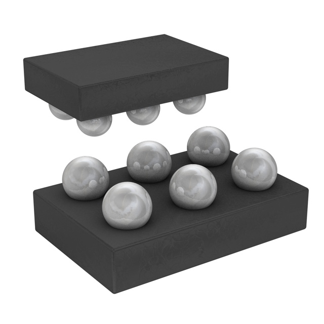
These parts are available in a space-saving 6-ball
2
advanced. Pb-Free 1.0 x1.5 mm CSP package.
Peripheral Ports
MP3 Players
Figure 1.
© 2008 Fairchild Semiconductor Corporation
FPF2024/25/26/27 • Rev. 1.1
2
6-Ball 1.0 x1.5 mm CSP Package
www.fairchildsemi.com
FPF2024/25/26/27 — Full Function Load Switch with 100 mA Current Limit
April 2016
�Blank Current
Auto-Restart
Limit Time
Time [ms]
[ms]
Part Number
Min. Limit
[mA]
ON Pin
Activity
FLAGB
Top Mark
FPF2024
100
10
70
Active HI
Open Drain
S2
FPF2025
100
10
70
Active LO
CMOS
S3
FPF2026
FPF2027
100
10
n/a
Active HI
Open Drain
S4
100
0
n/a
Active HI
Open Drain
S5
Typical Application
Figure 2.
Typical Application
Block Diagram
Figure 3.
© 2008 Fairchild Semiconductor Corporation
FPF2024/25/26/27 • Rev. 1.1
Block Diagram
www.fairchildsemi.com
2
PFPF2024/25/26/27 — Full Function Load Switch with 100 mA Current Limit
Ordering Information
�Figure 4.
Pin Assignment 1.0 x 1.5 CSP Bottom View
Pin Description
Pin
Name
A1
VOUT
A2
VIN
B1
GND
B2
NC
C1
FLAGB
C2
ON
Function
Switch Output. Output of the power switch.
Supply Input. Input to the power switch and the supply voltage for the IC.
Ground.
No Connection.
Fault Output. Active LOW, open drain output for PFPF2024/26/27 and CMOS output for
FPF2025. FLAGB indicates an over-current, supply under-voltage or over-temperature state.
ON/OFF Control Input. Active HIGH for FPF2024/26/27 and Active LOW for FPF2025.
© 2008 Fairchild Semiconductor Corporation
FPF2024/25/26/27 • Rev. 1.1
www.fairchildsemi.com
3
PFPF2024/25/26/27 — Full Function Load Switch with 100 mA Current Limit
Pin Configuration
�Stresses exceeding the absolute maximum ratings may damage the device. The device may not function or be
operable above the recommended operating conditions and stressing the parts to these levels is not recommended.
In addition, extended exposure to stresses above the recommended operating conditions may affect device reliability.
The absolute maximum ratings are stress ratings only.
Symbol
VIN
Parameter
VIN, VOUT, ON, FLAG, GND
Min.
Max.
Unit
-0.3
6.0
V
(1)
PD
Power Dissipation at TA=25°C
1.2
W
ISW
Maximum Continuous Switch Current
0.2
A
TA
Operating Temperature Range
-40
125
°C
TSTG
Storage Junction Temperature
-65
150
°C
JA
Thermal Resistance, Junction-to-Ambient
85
°C/W
ESD
Electrostatic Discharge Capability
Human Body Model
5500
Charged Device Model
1500
V
Note:
1. Package power dissipation on 1 square inch pad, 2 oz. copper board.
Recommended Operating Conditions
The Recommended Operating Conditions table defines the conditions for actual device operation. Recommended
operating conditions are specified to ensure optimal performance. Fairchild does not recommend exceeding them or
designing to Absolute Maximum Ratings.
Symbol
Parameter
Min.
Max.
Unit
VIN
Input Voltage
1.6
5.5
V
TA
Ambient Operating Temperature
-40
85
°C
© 2008 Fairchild Semiconductor Corporation
FPF2024/25/26/27 • Rev. 1.1
www.fairchildsemi.com
4
PFPF2024/25/26/27 — Full Function Load Switch with 100 mA Current Limit
Absolute Maximum Ratings
�Unless otherwise noted, VIN=1.6 to 5.5 V and TA=-40 to +85°C. Typical values are at VIN=3.3 V and TA=25°C.
Symbol
Parameter
Conditions
Min.
Typ.
Max.
Unit
5.5
V
4
μA
1
μA
Basic Operation
VIN
Operating Voltage
1.6
IQ
Quiescent Current
IOUT=0 mA, VON Active, VIN=1.8 V
(Average)
ISD
Shutdown Current
VON=VIN, (FPF2025) VON=GND
(FPF2024/26/27), IOUT=0
1
TA=25°C, VIN=5.5 V
TA=-40 to 85°C, VIN=5.5 V
RON
On Resistance
120
TA=25°C,VIN=3.3 V
TA= -40 to +85°C, VIN=3.3 V
140
TA= 25°C,VIN=1.6 V
VIH
On Input Logic HIGH Voltage
VIL
On Input Logic LOW Voltage
ION
ISWOFF
TA= -40 to +85°C, VIN=1.6 V
180
VIN=1.6 V
0.8
VIN=5.5 V
1.5
215
315
215
350
225
325
225
360
305
490
305
580
mΩ
V
VIN=1.6 V
0.45
VIN=5.5 V
0.9
On Input Leakage
VON=VIN or GND
1.0
μA
Off Switch Leakage
VON=VIN, VOUT=0 V
1.0
μA
FLAGB Output Logic Low Voltage
FLAGB Output Logic High Voltage
VIN=5.5 V, ISINK=1 mA
0.1
0.2
VIN=1.8 V, ISINK=1 mA
0.1
0.3
VIN=5.5 V, ISOURCE=1 mA, FPF2025
5.2
5.4
VIN=1.6 V, ISOURCE=1 mA, FPF2025
1.20
1.35
FLAGB Output High Leakage
Current
VIN=5.5 V, Switch On,
FPF2024, FPF2026, FPF2027
Current Limit
VIN=3.3 V, VOUT=3.0 V,TA=25°C
V
V
V
1.0
μA
200
mA
Protections
ILIM
Thermal Shutdown
100
140
Return from Shutdown
130
Hysteresis
UVLO
Under-Voltage Lockout
UVLOH
Under-Voltage Lockout Hysteresis
150
Shutdown Threshold TJ Increasing
°C
10
VIN Increasing
1.475
1.525
1.575
V
40
mV
Dynamic Characteristics
tON
Turn-On Time
RL = 500 Ω, CL = 0.1 μF
70
μs
μs
tOFF
Turn-Off Time
RL = 500 Ω
10
tRISE
VOUT Rise Time
RL = 500 Ω, CL = 0.1 μF
30
tBLANK
Over-Current Blanking Time
FPF2024, FPF2025, FPF2026
TSTART_BLANK Startup FLAGB Blanking Time
tRSTRT
Auto-Restart Time
5
10
FPF2027(2)
5
FPF2024, FPF2025
35
128.5
Sleep Mode Duration
Wake-up Mode Duration
0.5
μs
20
ms
10
20
ms
70
140
ms
257.0
514.0
ms
1.0
2.0
ms
Duty Cycle
Wake-up: Sleep Mode Duty Cycle
1:257
Current Limit Response Time
Moderate Over-Current Condition
RL= 5
15
Blanking/Auto-Restart Duty Ratio
tBLANK /tRSTRT (Internally Fixed)
FPF2024, FPF2025
1:7
μs
Note:
2. FPF2027 has a 10 ms Startup FLAGB Blanking Time when the part is turned on via ON pin to ensure transient
load currents settle down.
© 2008 Fairchild Semiconductor Corporation
FPF2024/25/26/27 • Rev. 1.1
www.fairchildsemi.com
5
PFPF2024/25/26/27 — Full Function Load Switch with 100 mA Current Limit
Electrical Characteristics
�Figure 5.
Shutdown Current vs. Temperature
Figure 6.
TRestart vs. Temperature
Figure 7.
Quiescent Current vs. Temperature
Figure 8.
TBlank vs. Temperature
Figure 10.
RDS(ON) vs. Temperature
Figure 9.
RDS(ON) vs. VIN
© 2008 Fairchild Semiconductor Corporation
FPF2024/25/26/27 • Rev. 1.1
www.fairchildsemi.com
6
PFPF2024/25/26/27 — Full Function Load Switch with 100 mA Current Limit
Typical Performance Characteristics
�PFPF2024/25/26/27 — Full Function Load Switch with 100 mA Current Limit
Typical Performance Characteristics (Continued)
Figure 11.
ILimit vs. VIN
Figure 13.
VIH, VIL vs. Temperature
Figure 15.
FPF2024 tOFF Response
© 2008 Fairchild Semiconductor Corporation
FPF2024/25/26/27 • Rev. 1.1
Figure 12.
Figure 14.
Figure 16.
ILimit vs. Temperature
FPF2024 tON Response
FPF2024 TBLANK Response
(3)
www.fairchildsemi.com
7
�Figure 17.
(3)
FPF2024 TRESTART Response
Figure 18. FPF2024 Current Limit Response Time
(Output is loaded by 5 Ω and COUT = 10 μF)
Figure 19. FPF2024 Current Limit Response Time
(Output is loaded by 5 Ω and COUT = 100 μF)
Figure 20. FPF2024 Short Circuit Response Time
(Output shorted to GND while the switch is in normal
operation)
Figure 21. FPF2024 Current Limit Response
(Input and enable pin are tied together and VOUT
is shorted to GND)
Figure 22. FPF2027 Over-Current
Over-Current condition is applied while device in
normal operation (FLAGB inserts immediately and
reports the fault condition)
© 2008 Fairchild Semiconductor Corporation
FPF2024/25/26/27 • Rev. 1.1
(3)
www.fairchildsemi.com
8
PFPF2024/25/26/27 — Full Function Load Switch with 100 mA Current Limit
Typical Performance Characteristics (Continued)
�Figure 23.
FPF2027 Startup FLAGB Blanking Time
Figure 24.
FPF2025 TBLANK and TRESTART
(Active LO Device)
Note:
3. VDRV signal forces the device to go into over-current condition by loading a 7.5 Ω.
© 2008 Fairchild Semiconductor Corporation
FPF2024/25/26/27 • Rev. 1.1
www.fairchildsemi.com
9
PFPF2024/25/26/27 — Full Function Load Switch with 100 mA Current Limit
Typical Performance Characteristics (Continued)
�FPF2024-FPF2027 series Full-Function switches are
current limited load switches with ultra-low power
consumption. The core of each device consists of a
230 mW P-channel MOSFET featuring slow turn-on to
limit the inrush current, fast turn-off, current limit, UnderVoltage Lockout (UVLO) and thermal shutdown
protection features and a FLAGB output that indicates
that a fault condition has occurred.
the OFF state when the ON pin is inactive. In addition,
FPF2026 moves into the OFF state if a current fault is
encountered for longer duration than the Blanking Time.
For all versions, an under-voltage on VIN or a junction
temperature in excess of 140°C overrides the ON
control and turns off the switch.
In addition, a current fault condition longer than the
Blanking Time will cause the switch to turn off in the
FPF2024, FPF2025 and FPF2026. The FPF2024 and
FPF2025 have an Auto-Restart feature which will
automatically turn the switch on again after 70 ms. For
the FPF2026, the ON pin must be toggled to turn the
switch on again. The FPF2027 does not turn off in
response to an over-current condition, and remains in a
constant current mode for so long as the ON pin is
active, and the thermal shutdown or UVLO are not
activated.
Some versions in the FPF202x series also feature
Current Limit Blanking and Auto-Restart.
The FPF202x family achieves an ultra-low current
consumption of 1 μA through a proprietary “Sleep and
Wake-up Modes” implementation. Full functionality is
guaranteed for operating voltages down to 1.6 V over
the -40°C to +85°C temperature range.
Sleep and Wakeup Mode Description
The ON pin control voltage and VIN pin have
independent recommended operating ranges. The ON
pin voltage can be driven by a voltage level higher than
the input voltage.
The ultra-low power consumption of FPF2024-FPF2027
is achieved through the implementation of proprietary
Sleep/ Wakeup modes.
The FPF2024-FPF2027 family turns on in Startup mode
where it checks for potential load current, temperature,
and under-voltage faults for 10 ms. If no faults are
detected during this startup period, the FPF2024FPF2027 goes into a Sleep mode where it stays for
257 ms. At the end of the Sleep period, the part goes
into Wakeup mode to check for any fault condition. If no
fault is detected in 1 ms, the part goes back to Sleep
mode. The 1:257 Wakeup/Sleep duty cycle results in an
overall average current consumption of 1 μA (typical).
Fault Reporting
Over-current, input under-voltage, or over-temperature
fault conditions are signaled out by the FLAGB pin going
low. FPF2024, FPF2025 and FPF2026 have a current
fault blanking feature which prevents current faults
lasting shorter than the Blanking Time of 10 ms (typical)
from triggering the fault signal (FLAGB) output.
If the over-current condition persists beyond the
Blanking Time, the FPF2024 and FPF2025 pull the
FLAGB pin low and shut the switch off. If the ON pin is
kept active, an Auto-Restart feature releases the
FLAGB pin and turns the switch on again after 70 ms.
During Sleep mode the thermal and under-voltage
conditions are not monitored to reduce the current
consumption of the device.
The switch current limiting circuitry is active at all times
and protects the FPF2024-FPF2027 against excessive
load currents in all modes. While in the Wakeup mode,
a current fault event will prevent the part from reentering into Sleep mode even if input voltage and
temperature faults are not present. In such a case, the
part functions according to its feature set, e.g., it
performs its normal Blanking, Auto-Restart or Latch-off
functions as expected. If the over-current condition is
removed from the output, the part will go back into
Sleep mode after 10ms. The representative state
diagrams of the FPF2024-FPF2027 are given in Figure
25, Figure 26 and Figure 27.
If the over-current condition persists beyond the
Blanking Time, the FPF2026 has a Latch-Off feature
which pulls the FLAGB pin low and shuts the switch off.
The switch is kept off and the FLAGB pin is kept low
until the ON pin is toggled.
The FPF2027 responds to an overload condition by
immediately pulling the FLAGB pin low and the switch
remains in constant current mode until the output
overload condition is removed. The FPF2027 has a
Startup Blanking feature which prevents current faults
related to startup transients from triggering the FLAGB
output. The Startup Blanking feature is effective for the
first 10 ms (typical) following device turn-on via ON pin.
The ultra-low quiescent current consumption of 1 μA
along with the very-low minimum operating voltage of
1.6 V, make the FPF2024-FPF2027 an ideal fullfunction load switch for ultraportable applications.
The FPF2024, FPF2026 and FPF2027 have an opendrain MOSFET FLAGB output which requires a pull-up
resistor between VIN and FLAGB. A 100 KΩ pull up
resistor is recommended. The FPF2025 has a CMOS
FLAGB output and does not require a pull-up resistor.
During shutdown, the pull-down on FLAGB is disabled
to reduce current draw from the supply.
On/Off Control
The ON pin controls the state of the switch. The
FPF2024- FPF2027 series features both active high and
low configurations to accommodate various application
requirements. FPF2024, FPF2026 and FPF2027 are
active high switches while the FPF2025 is an active low
device. Applying a continuous high or low signal
depending on the switch configuration, will hold the
switch in the ON state. The load switch will move into
© 2008 Fairchild Semiconductor Corporation
FPF2024/25/26/27 • Rev. 1.1
www.fairchildsemi.com
10
PFPF2024/25/26/27 — Full Function Load Switch with 100 mA Current Limit
Description of Operation
�Thermal Shutdown
The current limit function ensures that the current
through the switch does not exceed a maximum value
while not limiting at less than a minimum value. The
minimum current at which the parts will limit the load
current is internally set to 100 mA.
The Thermal Shutdown protects the device from
internally
or
externally
generated
excessive
temperatures. The Thermal shutdown feature is
disabled during Sleep mode. However, excessive load
currents that may result in high power dissipation will be
detected during Sleep mode and will activate the full
function Wakeup mode, which has thermal shutdown
protection. During an over-temperature condition the
FLAGB is pulled low and the switch is turned-off. If the
temperature of the die drops below the threshold
temperature, the switch automatically turns on again, To
avoid unwanted thermal oscillations, a 10°C (typical)
thermal hysteresis is implemented between thermal
shutdown entry and exit temperatures.
The switch current limiting circuitry is active at all times
(Sleep and Wakeup mode) and protects the FPF2024FPF2027 against excessive load currents in all modes.
The proprietary current limiting circuit responds to an
over-current condition in 15 μs (typical).
Under-Voltage Lockout (UVLO)
The under-voltage lockout feature turns-off the switch if
the input voltage drops below the under-voltage lockout
threshold. With the ON pin active, the input voltage
rising above the under-voltage lockout threshold will
cause a controlled turn-on of the switch and will limit
current over-shoots. The UVLO feature is disabled
during Sleep mode. If device is in the UVLO condition,
FLAGB goes low and indicates the fault. If the input
voltage goes below UVLO voltage but remains above
1.3 V (typical) during Sleep mode, the switch is kept on
until the next Wakeup cycle, where the UVLO violation
will be detected. If the input voltage falls below 1.3 V in
Sleep mode, the switch is immediately turned off.
Figure 25.
© 2008 Fairchild Semiconductor Corporation
FPF2024/25/26/27 • Rev. 1.1
State Diagram with Blanking and Auto-Restart (FPF2024/5)
www.fairchildsemi.com
11
PFPF2024/25/26/27 — Full Function Load Switch with 100 mA Current Limit
Current Limiting
�© 2008 Fairchild Semiconductor Corporation
FPF2024/25/26/27 • Rev. 1.1
PFPF2024/25/26/27 — Full Function Load Switch with 100 mA Current Limit
Figure 26.
State Diagram with Blanking Only (No Auto-Restart FPF2026)
www.fairchildsemi.com
12
�© 2008 Fairchild Semiconductor Corporation
FPF2024/25/26/27 • Rev. 1.1
PFPF2024/25/26/27 — Full Function Load Switch with 100 mA Current Limit
Figure 27.
State Diagram with No Blanking (FPF2027)
www.fairchildsemi.com
13
�This power dissipation is significant enough that it will
activate the thermal shutdown protection, and the part
will cycle in and out of thermal shutdown so long as the
ON pin is active and the output short is present.
Input Capacitor
To limit the voltage drop on the input supply caused by
transient in-rush currents when the switch is turned on
into a discharged load capacitor or a short-circuit, a
capacitor is recommended to be placed between V IN
and GND. The FPF2024-FPF2027 series feature a slow
turn-on to limit the inrush current and requires a smaller
input capacitor. A 1 µF ceramic capacitor, CIN, placed
close to the pins is typically sufficient. Higher values of
CIN can be used to further reduce the voltage drop.
Improving Thermal Performance
An improper layout could result in higher junction
temperature and ultimately trigger the thermal shutdown
protection feature. This concern applies particularly
significant for the FPF2027 where the switch is in
constant current mode in the overload conditions.
Output Capacitor
The following techniques have been identified to
improve the thermal performance of this family of
devices. These techniques are listed in order of the
significance of their impact.
A 0.1 µF capacitor COUT, should be placed between
VOUT and GND. This capacitor will prevent parasitic
board inductances from forcing VOUT below GND when
the switch turns-off. For the FPF2024, FPF2025 and
FPF2026, the total output capacitance needs to be kept
below a maximum value, COUT(MAX), to prevent the part
from registering an over-current condition beyond the
Blanking Time and turning-off the switch. The maximum
output capacitance can be determined from the
following formula:
NC pin can be connected to the GND plane to
improve thermal performance.
The VIN, VOUT and GND pins will dissipate most of
the heat generated during a high load current
condition. Using wide traces will help minimize
parasitic electrical effects, along with minimizing the
case to ambient thermal impedance. The layout
suggested in Figure 28 provides each pin with
adequate copper so that heat may be transferred
out of the device as efficiently as possible. The lowpower FLAGB and ON pin traces may be laid-out to
maximize the area available to the ground pad.
Placing the input and output capacitors as close to
the device as possible also contributes to heat
dissipation, particularly during high load currents.
(1)
Power Dissipation
During normal operation as a switch, the power
dissipation is small and has little effect on the operating
temperature of the part. The maximum power
dissipation while switch is in normal operation occurs
just before a part enters the current limit. This may be
calculated using the formula bellow:
FPF202X Demo Board
FPF202X Demo board has components and circuitry to
demonstrate the functions and features of the FPF202X
load switch family. An N-Channel MOSFET(Q), in series
with a 7.5 Ω resistor, are connected between VOUT and
the GND pin of the device. By turning on the Q
transistor, the 7.5 Ω is loaded to the output voltage and
simulates an over-current condition. The R2 resistor is
connected between FLAGB pin and input voltage as
pull-up resistor for FPF2024, FPF2026 and FPF2027
devices. The FPF2025 does not require a pull-up
resistor due to its CMOS output structure.
(2)
If the part goes into current limit, the maximum power
dissipation occurs when the output of switch is shorted
to ground. For the FPF2024 and FPF2025, the power
dissipation will scale with the Auto-Restart Time, tRSTRT,
and the Over Current Blanking Time, tBLANK. In this case
the maximum power dissipated for the FPF2024 and
FPF2025 is:
The thermal performance of the board is improved using
the
techniques
recommended
in
the
layout
recommendations section of datasheet.
(3)
Take note that this is below the maximum package
power dissipation, and the thermal shutdown feature
protection provides additional safety to protect the part
from damage due to excessive heating. The junction
temperature is only able to increase to the thermal
shutdown threshold. Once this temperature has been
reached, toggling ON will have no effect until the
junction temperature drops below the thermal shutdown
exit temperature. For the FPF2027, a short on the
output will cause the part to operate in a constant
current state dissipating a worst case power of:
Figure 28.
(4)
FPF2020X Proper Layout
Output of FPF2027 is shorted to GND.
© 2008 Fairchild Semiconductor Corporation
FPF2024/25/26/27 • Rev. 1.1
www.fairchildsemi.com
14
PFPF2024/25/26/27 — Full Function Load Switch with 100 mA Current Limit
Application Information
�Top Layer
Figure 31.
Figure 30.
SST
Figure 32.
PFPF2024/25/26/27 — Full Function Load Switch with 100 mA Current Limit
Figure 29.
Bottom Layer
TOP, SST and SMT
The information below pertains to the WLCSP outline drawing on the following page.
Product Specifications
Product
D
E
X
Y
FPF2024/5/6/7
1.500 ±0.030
1.000 ±0.030
0.240
0.240
© 2008 Fairchild Semiconductor Corporation
FPF2024/25/26/27 • Rev. 1.1
www.fairchildsemi.com
15
�0.03 C
E
2X
F
A
(Ø0.250)
Cu Pad
(Ø0.350)
SOLDER MASK
OPENING
B
A1
(1.00)
BALL A1
INDEX AREA
D
(0.50)
0.03 C
2X
TOP VIEW
RECOMMENDED LAND PATTERN
(NSMD PAD TYPE)
0.06 C
0.625
0.539
0.05 C
C
0.332±0.018
0.250±0.025
E
SEATING PLANE
D
SIDE VIEWS
NOTES:
A. NO JEDEC REGISTRATION APPLIES.
0.005
Ø0.315 +/- .025
6X
0.50
C
1.00
B
A
0.50
(Y) ±0.018
1 2
F
(X) ±0.018
BOTTOM VIEW
C A B
B. DIMENSIONS ARE IN MILLIMETERS.
C. DIMENSIONS AND TOLERANCE
PER ASMEY14.5M, 1994.
D. DATUM C IS DEFINED BY THE SPHERICAL
CROWNS OF THE BALLS.
E. PACKAGE NOMINAL HEIGHT IS 582 MICRONS
±43 MICRONS (539-625 MICRONS).
F. FOR DIMENSIONS D, E, X, AND Y SEE
PRODUCT DATASHEET.
G. DRAWING FILNAME: MKT-UC006AFrev3.
�ON Semiconductor and
are trademarks of Semiconductor Components Industries, LLC dba ON Semiconductor or its subsidiaries in the United States and/or other countries.
ON Semiconductor owns the rights to a number of patents, trademarks, copyrights, trade secrets, and other intellectual property. A listing of ON Semiconductor’s product/patent
coverage may be accessed at www.onsemi.com/site/pdf/Patent−Marking.pdf. ON Semiconductor reserves the right to make changes without further notice to any products herein.
ON Semiconductor makes no warranty, representation or guarantee regarding the suitability of its products for any particular purpose, nor does ON Semiconductor assume any liability
arising out of the application or use of any product or circuit, and specifically disclaims any and all liability, including without limitation special, consequential or incidental damages.
Buyer is responsible for its products and applications using ON Semiconductor products, including compliance with all laws, regulations and safety requirements or standards,
regardless of any support or applications information provided by ON Semiconductor. “Typical” parameters which may be provided in ON Semiconductor data sheets and/or
specifications can and do vary in different applications and actual performance may vary over time. All operating parameters, including “Typicals” must be validated for each customer
application by customer’s technical experts. ON Semiconductor does not convey any license under its patent rights nor the rights of others. ON Semiconductor products are not
designed, intended, or authorized for use as a critical component in life support systems or any FDA Class 3 medical devices or medical devices with a same or similar classification
in a foreign jurisdiction or any devices intended for implantation in the human body. Should Buyer purchase or use ON Semiconductor products for any such unintended or unauthorized
application, Buyer shall indemnify and hold ON Semiconductor and its officers, employees, subsidiaries, affiliates, and distributors harmless against all claims, costs, damages, and
expenses, and reasonable attorney fees arising out of, directly or indirectly, any claim of personal injury or death associated with such unintended or unauthorized use, even if such
claim alleges that ON Semiconductor was negligent regarding the design or manufacture of the part. ON Semiconductor is an Equal Opportunity/Affirmative Action Employer. This
literature is subject to all applicable copyright laws and is not for resale in any manner.
PUBLICATION ORDERING INFORMATION
LITERATURE FULFILLMENT:
Literature Distribution Center for ON Semiconductor
19521 E. 32nd Pkwy, Aurora, Colorado 80011 USA
Phone: 303−675−2175 or 800−344−3860 Toll Free USA/Canada
Fax: 303−675−2176 or 800−344−3867 Toll Free USA/Canada
Email: orderlit@onsemi.com
© Semiconductor Components Industries, LLC
N. American Technical Support: 800−282−9855 Toll Free
USA/Canada
Europe, Middle East and Africa Technical Support:
Phone: 421 33 790 2910
Japan Customer Focus Center
Phone: 81−3−5817−1050
www.onsemi.com
1
ON Semiconductor Website: www.onsemi.com
Order Literature: http://www.onsemi.com/orderlit
For additional information, please contact your local
Sales Representative
www.onsemi.com
�