Is Now Part of
To learn more about ON Semiconductor, please visit our website at
www.onsemi.com
Please note: As part of the Fairchild Semiconductor integration, some of the Fairchild orderable part numbers
will need to change in order to meet ON Semiconductor’s system requirements. Since the ON Semiconductor
product management systems do not have the ability to manage part nomenclature that utilizes an underscore
(_), the underscore (_) in the Fairchild part numbers will be changed to a dash (-). This document may contain
device numbers with an underscore (_). Please check the ON Semiconductor website to verify the updated
device numbers. The most current and up-to-date ordering information can be found at www.onsemi.com. Please
email any questions regarding the system integration to Fairchild_questions@onsemi.com.
ON Semiconductor and the ON Semiconductor logo are trademarks of Semiconductor Components Industries, LLC dba ON Semiconductor or its subsidiaries in the United States and/or other countries. ON Semiconductor owns the rights to a number
of patents, trademarks, copyrights, trade secrets, and other intellectual property. A listing of ON Semiconductor’s product/patent coverage may be accessed at www.onsemi.com/site/pdf/Patent-Marking.pdf. ON Semiconductor reserves the right
to make changes without further notice to any products herein. ON Semiconductor makes no warranty, representation or guarantee regarding the suitability of its products for any particular purpose, nor does ON Semiconductor assume any liability
arising out of the application or use of any product or circuit, and specifically disclaims any and all liability, including without limitation special, consequential or incidental damages. Buyer is responsible for its products and applications using ON
Semiconductor products, including compliance with all laws, regulations and safety requirements or standards, regardless of any support or applications information provided by ON Semiconductor. “Typical” parameters which may be provided in ON
Semiconductor data sheets and/or specifications can and do vary in different applications and actual performance may vary over time. All operating parameters, including “Typicals” must be validated for each customer application by customer’s
technical experts. ON Semiconductor does not convey any license under its patent rights nor the rights of others. ON Semiconductor products are not designed, intended, or authorized for use as a critical component in life support systems or any FDA
Class 3 medical devices or medical devices with a same or similar classification in a foreign jurisdiction or any devices intended for implantation in the human body. Should Buyer purchase or use ON Semiconductor products for any such unintended
or unauthorized application, Buyer shall indemnify and hold ON Semiconductor and its officers, employees, subsidiaries, affiliates, and distributors harmless against all claims, costs, damages, and expenses, and reasonable attorney fees arising out
of, directly or indirectly, any claim of personal injury or death associated with such unintended or unauthorized use, even if such claim alleges that ON Semiconductor was negligent regarding the design or manufacture of the part. ON Semiconductor
is an Equal Opportunity/Affirmative Action Employer. This literature is subject to all applicable copyright laws and is not for resale in any manner.
�FPF3488
SIDO Over-Voltage Protection Load Switch
Features
Description
Single Input Dual Output (SIDO) Switch
VBUS to VOUT Path
VBUS to SYS Path
The FPF3488 features a Single Input Dual Output
(SIDO) power switch, which offers surge protection and
Over-Voltage Protection (OVP), to protect downstream
components and enhancing overall system robustness.
Surge Protection under IEC 61000-4-5
VBUS: ±100 V
Input Voltage Range
VBUS: 2.7 V ~ 13.5 V
Max. Continuous Current Capability
VOUT Path: 3.5 A
SYS Path: 6 A
VOUT Path: Typ. 28 mΩ
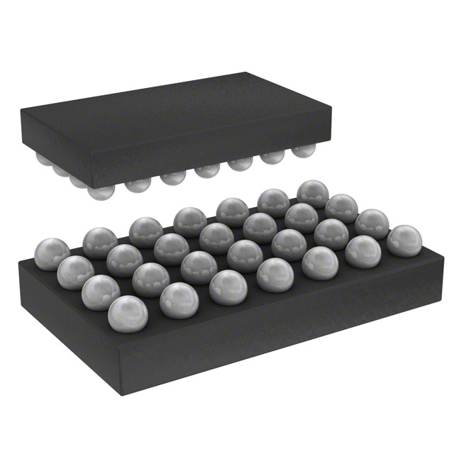
The FPF3488 is available in a 28-bump, 1.67 mm x
2.96 mm Wafer-Level Chip-Scale Package (WL-CSP)
with 0.4 mm pitch.
SYS Path: Typ. 33 mΩ
Over-Voltage Protection (OVP)
POK is paired with always ON LDO to power
downstream devices when VBUS is greater than 2.7 V,
regardless of OVLO, EN1 and EN2 State. This provides
system power supply without battery.
Ultra Low On-Resistance
-
Channel one (VBUS to VOUT) is an active-low, 28 V/3.5 A
rated, power MOSFET switch with an internal clamp
supporting ±100 V surge protection, fixed OVP at 13.9 V
(±400 mV). Channel two (VBUS to SYS) is a active-high,
6 V/6 A rated, power MOSFET, fixed OVP at 5.25 V
(±250 mV) and Reverse Current Blocking (RCB) during
its OFF State.
VOUT Path: 13.9 V ±400 mV
Applications
SYS Path: 5.25 V ±250 mV
Always ON LDO Output POK for VBUS Detection
and System Power Up without Battery
Mobile Handsets and Tablets
Wearable Devices
Active LOW Control for VBUS to VOUT Path
Active HIGH Control for VBUS to SYS Path
Active HIGH Control for Device Shutdown
CMOS output FLAG for VBUS to SYS Path
Additional Information
For the full datasheet, please contact a Fairchild
Sales Representative.
RCB for VBUS to SYS Path
Over-Temperature Protection (OTP)
Ordering Information
Part Number
Operating Temperature
Top Mark
Range
FPF3488UCX
-40°C – +85°C
VE
Packing
Method
Package
28-Ball, 0.4 mm Pitch WLCSP
Tape & Reel
Product-Specific Dimensions
This table applies to the WLCSP package dimensions on the following page.
D
E
X
Y
2960 μm ±30 μm
1670 μm ±30 μm
235 μm ±18 μm
280 μm ±18 μm
© 2015 Fairchild Semiconductor Corporation
FPF3488 • 1.4
www.fairchildsemi.com
FPF3488 — SIDO Over-Voltage Protection Load Switch
August 2015
�0.03 C
E
2X
F
A
1.20
B
0.40
A1
BALL A1
INDEX AREA
Solder Mask
2.40
D
Bottom of Cu Pad
0.40
0.03 C
TOP VIEW
RECOMMENDED LAND PATTERN
(NSMD PAD TYPE)
2X
0.06 C
0.05 C
E
C
D
SEATING PLANE
1.20
0.005
0.40
28X
G
F
E
2.40
A
1 2 3 4
F
BOTTOM VIEW
C A B
NOTES
A. NO JEDEC REGISTRATION APPLIES.
B. DIMENSIONS ARE IN MILLIMETERS.
C. DIMENSIONS AND TOLERANCE
PER ASMEY14.5M, 2009.
D. DATUM C IS DEFINED BY THE SPHERICAL
CROWNS OF THE BALLS.
E. PACKAGE NOMINAL HEIGHT IS
F. FOR DIMENSIONS D, E, X, AND Y SEE
PRODUCT DATASHEET.
G. DRAWING FILENAME: MKT-UC028AB REV1.
D
C
B
0.40
SIDE VIEWS
�ON Semiconductor and
are trademarks of Semiconductor Components Industries, LLC dba ON Semiconductor or its subsidiaries in the United States and/or other countries.
ON Semiconductor owns the rights to a number of patents, trademarks, copyrights, trade secrets, and other intellectual property. A listing of ON Semiconductor’s product/patent
coverage may be accessed at www.onsemi.com/site/pdf/Patent−Marking.pdf. ON Semiconductor reserves the right to make changes without further notice to any products herein.
ON Semiconductor makes no warranty, representation or guarantee regarding the suitability of its products for any particular purpose, nor does ON Semiconductor assume any liability
arising out of the application or use of any product or circuit, and specifically disclaims any and all liability, including without limitation special, consequential or incidental damages.
Buyer is responsible for its products and applications using ON Semiconductor products, including compliance with all laws, regulations and safety requirements or standards,
regardless of any support or applications information provided by ON Semiconductor. “Typical” parameters which may be provided in ON Semiconductor data sheets and/or
specifications can and do vary in different applications and actual performance may vary over time. All operating parameters, including “Typicals” must be validated for each customer
application by customer’s technical experts. ON Semiconductor does not convey any license under its patent rights nor the rights of others. ON Semiconductor products are not
designed, intended, or authorized for use as a critical component in life support systems or any FDA Class 3 medical devices or medical devices with a same or similar classification
in a foreign jurisdiction or any devices intended for implantation in the human body. Should Buyer purchase or use ON Semiconductor products for any such unintended or unauthorized
application, Buyer shall indemnify and hold ON Semiconductor and its officers, employees, subsidiaries, affiliates, and distributors harmless against all claims, costs, damages, and
expenses, and reasonable attorney fees arising out of, directly or indirectly, any claim of personal injury or death associated with such unintended or unauthorized use, even if such
claim alleges that ON Semiconductor was negligent regarding the design or manufacture of the part. ON Semiconductor is an Equal Opportunity/Affirmative Action Employer. This
literature is subject to all applicable copyright laws and is not for resale in any manner.
PUBLICATION ORDERING INFORMATION
LITERATURE FULFILLMENT:
Literature Distribution Center for ON Semiconductor
19521 E. 32nd Pkwy, Aurora, Colorado 80011 USA
Phone: 303−675−2175 or 800−344−3860 Toll Free USA/Canada
Fax: 303−675−2176 or 800−344−3867 Toll Free USA/Canada
Email: orderlit@onsemi.com
© Semiconductor Components Industries, LLC
N. American Technical Support: 800−282−9855 Toll Free
USA/Canada
Europe, Middle East and Africa Technical Support:
Phone: 421 33 790 2910
Japan Customer Focus Center
Phone: 81−3−5817−1050
www.onsemi.com
1
ON Semiconductor Website: www.onsemi.com
Order Literature: http://www.onsemi.com/orderlit
For additional information, please contact your local
Sales Representative
www.onsemi.com
�