8 A Standard Recovery
Surface Mount Rectifiers
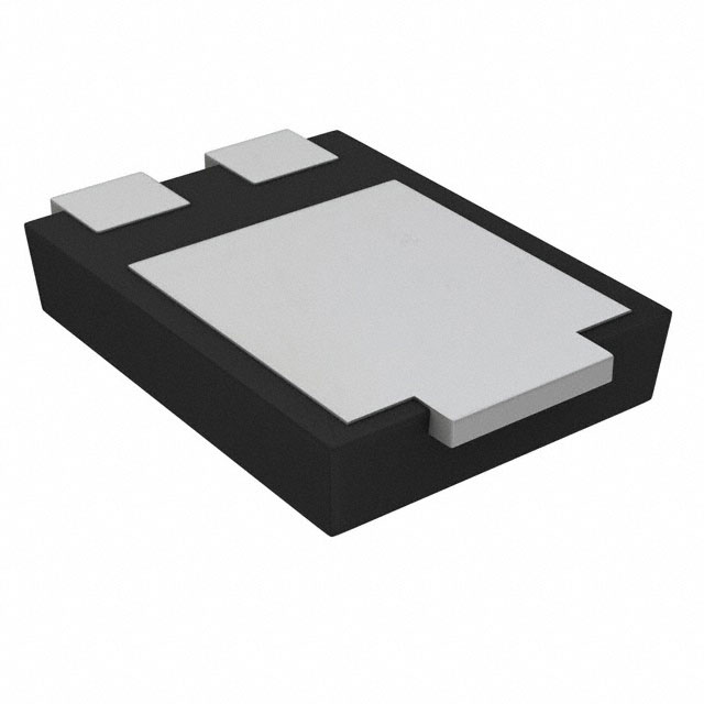
FS8G - FS8M
Description
The FS8G to FS8M series offers breakthrough size and
performance. It sinks 8 A DC forward current and provides up to
230 A surge current capability with only 0.37 mA reverse leakage
current. All this capability is packed into a small, flat−lead, TO−277
package, optimized for space−constrained applications.
www.onsemi.com
Anode 1
3
Cathode
Features
•
•
•
•
•
•
•
•
Anode 2
Rectifier
Very High forward Surge Capability: IFSM = 230 A
Low Leakage Current: 0.37 mA at TA = 25°C
Very Low Profile: Typical Height of 1.1 mm
Glass Passivated Junction
HBM (JEDEC A114) > 8 KV; CDM (JEDEC C101C) > 2 KV
Green Molding Compound as per IEC61249 Standard
With DAP Option Only
These Devices are Pb−Free, Halogen Free Free and are RoHS
Compliant
3
2
1
TO−277−3LD
CASE 340BQ
MARKING DIAGRAM
Applications
• General−Purpose Applications
• Reverse Polarity Protection
• Rectifications
$Y&Z&3
*
$Y
&Z
&3
*
= ON Semiconductor Logo
= Assembly Plant Code
= Date Code (Year & Week)
= Specific Device Code
FS8G, FS8J, FS8K, FS8M
ORDERING INFORMATION
See detailed ordering and shipping information on page 3 of
this data sheet.
© Semiconductor Components Industries, LLC, 2015
April, 2020 − Rev. 5
1
Publication Order Number:
FS8M/D
�FS8G − FS8M
ABSOLUTE MAXIMUM RATINGS (TA = 25°C unless otherwise noted)
Value
Symbol
Rating
FS8G
FS8J
FS8K
FS8M
Unit
600
800
1000
V
VRRM
Maximum Repetitive Peak Reverse Voltage
400
VRMS
Maximum RMS Reverse Voltage
280
420
560
700
V
VDC
DC Blocking Voltage
400
600
800
1000
V
IF(AV)
Maximum Average Rectified Forward Current
IFSM
Peak Forward Surge Current: 8.3 ms Single Half
Sine−Wave Superimposed on Rated Load
TJ
TSTG
8
A
230
A
Operating Junction Temperature Range
−55 to +150
°C
Storage Temperature Range
−55 to +150
°C
Stresses exceeding those listed in the Maximum Ratings table may damage the device. If any of these limits are exceeded, device functionality
should not be assumed, damage may occur and reliability may be affected.
THERMAL CHARACTERISTICS (TA = 25°C unless otherwise noted) (Note 1)
Symbol
Characteristic
Minimum
Land Pattern
Maximum
Land Pattern
Unit
RqJA
Junction−to−Ambient Thermal Resistance
100
40
°C/W
ΨJL
Junction−to−Lead Thermal Characteristics, Thermocouple Soldered to Anode
20
12
°C/W
Junction−to−Lead Thermal Characteristics, Thermocouple Soldered to Cathode
6
5
1. The thermal resistances (RqJA & ΨJL) are characterized with device mounted on the following FR4 printed circuit boards, as shown in Figure 1
and Figure 2. PCB size: 76.2 x 114.3 mm. Minimum land pattern size: 4.9 x 4.8 mm (big pattern, x1), 1.4 x 1.52 mm (small pattern, x2).
Maximum land pattern size: 30 x 30 mm (pattern, x2). Force line trace size = 55 mils, sense line trace size = 4 mils.
F
S
F
S
F
S
F
S
F
S
Figure 1. Minimum Land Pattern of 2 oz Copper
Figure 2. Maximum Land Pattern of 2 oz Copper
ELECTRICAL CHARACTERISTICS (TA = 25°C unless otherwise noted)
Symbol
VF
Parameter
Forward Voltage
Conditions
IF = 8 A
Min
Typ
Max
Unit
−
0.951
1.1
V
5
mA
IF = 8 A, TA = 125°C
IR
DC Reverse Current
0.845
−
VR = VDC
VR = VDC, TA = 125°C
0.37
84
Trr
Reverse Recovery Time
IF = 0.5 A, IR = 1 A, Irr = 0.25 A
3.37
ms
CJ
Junction Capacitance
VR = 0 V, f = 1 MHz
118
pF
Product parametric performance is indicated in the Electrical Characteristics for the listed test conditions, unless otherwise noted. Product
performance may not be indicated by the Electrical Characteristics if operated under different conditions.
www.onsemi.com
2
�FS8G − FS8M
ORDERING INFORMATION
Part Number
Top Mark
Package
Shipping†
FS8G
FS8G
TO−277 3L
(No DAP Option)
(Pb−Free/Halogen Free)
5000 / Tape & Reel
FS8J
FS8J
TO−277 3L
(No DAP Option)
(Pb−Free/Halogen Free)
5000 / Tape & Reel
FS8K
FS8K
TO−277 3L
(No DAP Option)
(Pb−Free/Halogen Free)
5000 / Tape & Reel
FS8M
FS8M
TO−277 3L
(No DAP Option)
(Pb−Free/Halogen Free)
5000 / Tape & Reel
†For information on tape and reel specifications, including part orientation and tape sizes, please refer to our Tape and Reel Packaging
Specifications Brochure, BRD8011/D.
www.onsemi.com
3
�FS8G − FS8M
TYPICAL PERFORMANCE CHARACTERISTICS
1000
TL (Cathode, Min. Pad)
8
CJ, Junction Capacitance (pF)
IF, Average Forward Current (A)
9
7
6
5
TA (3 cm x 3 cm Pad)
4
3
TA (Min. Pad)
2
1
100
0
0
25
50
75
100
150
10
0.1
175
1
10
100
Ambient / Lead Temperature (5C)
VR, Reverse Voltage (V)
Figure 3. Forward Current Derating Curve
Figure 4. Typical Junction Capacitance
1000
TA = 150°C
TA = 75°C
100
TA = 125°C
10
TA = 75°C
1
0.1
10
IF, Forward Current (A)
IR, Reverse Current (mA)
125
TA = 25°C
0.01
TA = 125°C
TA = 150°C
TA = 25°C
TA = −55°C
TA = −55°C
1E−3
0
1
0.5
100 200 300 400 500 600 700 800 900 1000
0.7
0.8
0.9
1.0
1.1
1.2
VR, Reverse Voltage (V)
VF, Forward Voltage (V)
Figure 5. Typical Reverse Characteristics
Figure 6. Typical Forward Characteristics
300
10000
IFSM, Non−Repetitive Forward
Surge Current (A)
Peak Forward Surge Current (A)
0.6
250
200
150
100
50
0
1
10
1000
100
100
10
Number of Cycles
100
1000
10000
Tp, Square Waveform Pulse Duration (ms)
NOTE:
Figure 7. Maximum Non−Repetitive Peak
Forward Surge Current
Typical performance bases on a limited sample
size, not guarantee rating.
Figure 8. Typical Non−Repetitive Forward Surge
Current
www.onsemi.com
4
�MECHANICAL CASE OUTLINE
PACKAGE DIMENSIONS
TO−277−3LD
CASE 340BQ
ISSUE O
DOCUMENT NUMBER:
DESCRIPTION:
98AON13861G
TO−277−3LD
DATE 30 SEP 2016
Electronic versions are uncontrolled except when accessed directly from the Document Repository.
Printed versions are uncontrolled except when stamped “CONTROLLED COPY” in red.
PAGE 1 OF 1
ON Semiconductor and
are trademarks of Semiconductor Components Industries, LLC dba ON Semiconductor or its subsidiaries in the United States and/or other countries.
ON Semiconductor reserves the right to make changes without further notice to any products herein. ON Semiconductor makes no warranty, representation or guarantee regarding
the suitability of its products for any particular purpose, nor does ON Semiconductor assume any liability arising out of the application or use of any product or circuit, and specifically
disclaims any and all liability, including without limitation special, consequential or incidental damages. ON Semiconductor does not convey any license under its patent rights nor the
rights of others.
© Semiconductor Components Industries, LLC, 2019
www.onsemi.com
�onsemi,
, and other names, marks, and brands are registered and/or common law trademarks of Semiconductor Components Industries, LLC dba “onsemi” or its affiliates
and/or subsidiaries in the United States and/or other countries. onsemi owns the rights to a number of patents, trademarks, copyrights, trade secrets, and other intellectual property.
A listing of onsemi’s product/patent coverage may be accessed at www.onsemi.com/site/pdf/Patent−Marking.pdf. onsemi reserves the right to make changes at any time to any
products or information herein, without notice. The information herein is provided “as−is” and onsemi makes no warranty, representation or guarantee regarding the accuracy of the
information, product features, availability, functionality, or suitability of its products for any particular purpose, nor does onsemi assume any liability arising out of the application or use
of any product or circuit, and specifically disclaims any and all liability, including without limitation special, consequential or incidental damages. Buyer is responsible for its products
and applications using onsemi products, including compliance with all laws, regulations and safety requirements or standards, regardless of any support or applications information
provided by onsemi. “Typical” parameters which may be provided in onsemi data sheets and/or specifications can and do vary in different applications and actual performance may
vary over time. All operating parameters, including “Typicals” must be validated for each customer application by customer’s technical experts. onsemi does not convey any license
under any of its intellectual property rights nor the rights of others. onsemi products are not designed, intended, or authorized for use as a critical component in life support systems
or any FDA Class 3 medical devices or medical devices with a same or similar classification in a foreign jurisdiction or any devices intended for implantation in the human body. Should
Buyer purchase or use onsemi products for any such unintended or unauthorized application, Buyer shall indemnify and hold onsemi and its officers, employees, subsidiaries, affiliates,
and distributors harmless against all claims, costs, damages, and expenses, and reasonable attorney fees arising out of, directly or indirectly, any claim of personal injury or death
associated with such unintended or unauthorized use, even if such claim alleges that onsemi was negligent regarding the design or manufacture of the part. onsemi is an Equal
Opportunity/Affirmative Action Employer. This literature is subject to all applicable copyright laws and is not for resale in any manner.
PUBLICATION ORDERING INFORMATION
LITERATURE FULFILLMENT:
Email Requests to: orderlit@onsemi.com
onsemi Website: www.onsemi.com
◊
TECHNICAL SUPPORT
North American Technical Support:
Voice Mail: 1 800−282−9855 Toll Free USA/Canada
Phone: 011 421 33 790 2910
Europe, Middle East and Africa Technical Support:
Phone: 00421 33 790 2910
For additional information, please contact your local Sales Representative
�