FSA1153
DP3T USB Type C Audio
and�UART Analog Switch
with OVP
Description
The FSA1153 is a bi−directional, low power, high speed USB2.0
Type−C, Audio and UART analog switch with overvoltage protection.
It is configured as a Double−Pole, Triple Throw (DP3T) switch. The
FSA1153s protection function prevents damage to Type−C USB 2.0
port pins caused by high voltage. It provides a receptacle side OVP
function on the USB 2.0 data pins and will turn off the relative switch
once the voltage level on DN_L or DP_R exceed the OV threshold. It
can withstand up to 20.5 V DC.
•
•
•
•
•
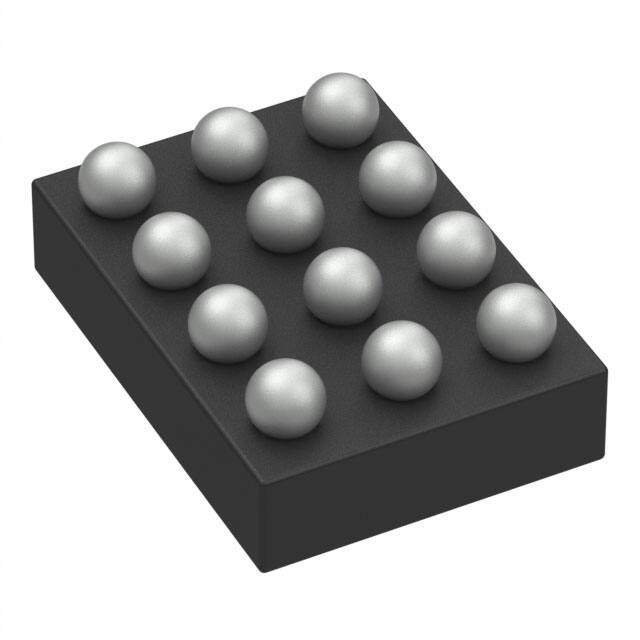
WLCSP12
CASE 567WM
MARKING DIAGRAM
Features
•
•
•
•
www.onsemi.com
DP3T USB Type C Audio and UART Analog Switch
VDD: 2.7 V to 5.5 V
ICC: 35 mA Typical
USB Switch
♦ −3 dB Bandwidth (Sdd21): 850 MHz
Audio Switch:
♦ Negative Rail Capability: −3 V to +3 V
♦ Audio Path RON = 1 W (Typ.) at 3.3 V
♦ THD + N = −110 dB; 1 VRMS, 32 W Load; f = 20 Hz ~ 20 kHz
with A−Weighted Filter
UART Switch:
♦ RON: 5 W (Typ.) at 3.3 V
♦ Signal Range: 0 − 4.4 V
High Power Supply Ripple Rejection
20.5 V Overvoltage Protection on DN_L/DP_R
20.5 V Surge Protection on DN_L/DP_R
6GKK
XYZ
6G
KK
X
Y
Z
= Device Number
= Assembly Lot
= Year
= Work Week
= Assembly Location
ORDERING INFORMATION
See detailed ordering and shipping information on page 3 of
this data sheet.
Applications
•
•
•
•
Mobile Phones
Tablets
Notebook PC
Media Player
© Semiconductor Components Industries, LLC, 2016
December, 2018 − Rev. 1
1
Publication Order Number:
FSA1153/D
�FSA1153
Typical Application
USB Type−C Receptacle
VDD
S0
GPIO 0
Logic
Control
S1
GPIO 1
GND
AP
USB D−
DN
USB D+
L
DN_L
RXD
AUX−
SSTXp1
SSRXn1
SSTXn1
VBUS
VBUS
SBU2
DN
CC1
DP
AUX+
DP
R
DP_R
TXD
L
R
SBU1
VBUS
SSTXn2
SSRXn2
SSTXp2
SSRXp2
Figure 1. Typical Application
Pin Definitions
DN
DP
TXD
B
DN_L
DP_R
RXD
C
L
R
S0
D
GND
VDD
S1
1
2
3
Figure 2. Top Through View
PIN DESCRIPTION
Pin
Name
A1
DN
USB Data (Differential –)
A2
DP
USB Data (Differential +)
A3
TXD
UART Transmit Data
B1
DN_L
USB/Audio/UART Common Connector
B2
DP_R
USB/Audio/UART Common Connector
B3
RXD
UART Receive Data
C1
L
Audio – Left Channel
C2
R
Audio – Right Channel
C3
S0
Data Switch Select
D1
GND
Chip Ground
D2
VDD
Power Supply (2.7 to 5.5 V)
D3
S1
Description
Data Switch Select
www.onsemi.com
2
DN
VBUS
GND
A
DP
CC2
GND
CODEC
GND
SSRXp1
GND
�FSA1153
Table 1. CONTROL LOGIC STATUS
S1
S0
USB Switch
Audio Switch
UART Switch
0
0
ON
OFF
OFF
0
1
OFF
ON
OFF
1
0
OFF
OFF
ON
1
1
Disable
Disable
Disable
ORDERING INFORMATION
Part Number
Operating
Temperature Range
FSA1153UCX
−40 to +85°C
Package
Top Mark
12−Ball WLCSP, Non−JEDEC
1.45 mm x 1.615 mm, 0.4 mm Pitch
6G
†For information on tape and reel specifications, including part orientation and tape sizes, please refer to our Tape and Reel Packaging
Specifications Brochure, BRD8011/D.
ABSOLUTE MAXIMUM RATINGS
Symbol
Min.
Max.
Unit
Supply Voltage from VDD
−0.5
6.5
V
VDP_R to GND, VDN_L to GND (Note 1)
−3.6
20.5
V
VSW_USB
VDP to GND, VDN to GND (Note 1)
−0.5
6.5
V
VDD
VSW_C
Parameter
VSW_Audio
VL to GND, VR to GND (Note 1)
−3.6
6.5
V
VSW_UART
VTXD to GND, VRXD to GND (Note 1)
−0.5
6.5
V
VSW
Control Input Voltage: S1, S0 (Note 2)
−0.5
6.5
V
ISW_Audio
Switch I/O Current, Audio path: R, L, DP_R, DN_L
−250
250
mA
ISW_USB
Switch I/O Current, USB path; DP to DP_R, DN to DN_L
−
100
mA
ISW_UART
Switch I/O Current, UART path; TXD to DP_R, RXD to DN_L
−
50
mA
IIK
ESD
DC Input Diode Current
−50
−
mA
Connector side and power pins: VDD, DP_R, DN_L
4
−
kV
Host side pins: The rest pins
2
−
1
−
−20.5
+20.5
V
Absolute Maximum Operating Temperature
−40
+85
°C
Storage Temperature
−65
+150
°C
Human Body Model,
ANSI / ESDA / JEDEC JS−001−2012
Charged Device Model, JEDEC: JESD22−C101
Surge
TA
TSTG
IEC 61000−4−5 System
Connector side pins: DP_R, DN_L
Stresses exceeding those listed in the Maximum Ratings table may damage the device. If any of these limits are exceeded, device functionality
should not be assumed, damage may occur and reliability may be affected.
1. The input and output negative ratings may be exceeded if the input and output diode current ratings are observed.
2. VSW refers to analog data switch paths.
www.onsemi.com
3
�FSA1153
RECOMMENDED OPERATING CONDITIONS
Symbol
Parameter
Min
Typ
Max
Unit
2.7
−
5.5
V
0
−
4.5
V
−3.0
−
+3.0
V
0
−
4.4
V
−40
25
+85
°C
POWER
VDD
Supply Voltage
USB SWITCH
VSW_USB
VDP to GND, VDN to GND, VDP_R to GND, VDN_L to GND
AUDIO SWITCH
VSW_Audio
VDP_R to GND, VDN_L to GND, VL to GND, VR to GND,
UART SWITCH
VSW_UART
VTXD to GND, VRXD to GND
OPERATING TEMPERATURE
TA
Ambient Operating Temperature
CONTROL VOLTAGE (S1, S0)
VIH
Input Voltage High
1.3
−
VCC
V
VIL
Input Voltage Low
0
−
0.5
V
Functional operation above the stresses listed in the Recommended Operating Ranges is not implied. Extended exposure to stresses beyond
the Recommended Operating Ranges limits may affect device reliability.
www.onsemi.com
4
�FSA1153
DC AND TRANSIENT CHARACTERISTICS
(VDD = 2.7 V to 5.5 V. VDD(Typ.) = 3.3 V, TA = −40°C to 85°C, and TA (Typ.) = 25°C, unless otherwise specified)
TA = −405C to 855C
Parameter
Symbol
Condition
Power
Min
Typ
Max
Unit
VDD: 2.7 to 5.5
−
−
35
mA
GENERAL DEVICE PINS
ICC
Supply current
For all switches
ICCZ
Quiescent current
S0, 1 = 1
−
−
3
Vin = 1.5 V
−
10
−
mA
ICCT
COMMON PINS: DP_R, DN_L
IOZ
Off leakage current of Port DP_R and DN_L
DP_R, DN_L = −3 V to 4.0 V
VDD: 2.7 to 5.5
−3.0
0.1
3.0
mA
IOFF
Power−Off leakage current of Port DP_R and
DN_L
DP_R, DN_L = 0 V to 4.0 V
Power off
−3.0
0.1
3.0
mA
Sweep from 3 V to 6 V
VDD: 2.7 to 5.5
4.7
5.0
5.3
V
VDD: 2.7 to 5.5
0.2
0.3
0.4
V
VOV_TRIP Input OVP Lockout
VOV_HYS
Input OVP Hysteresis
AUDIO SWITCH
ION
On leakage current of Audio switch
DN_L, DP_R = −3 V to 3.0 V,
R, L = Float
VDD: 2.7 to 5.5
−2.0
0.1
2.0
mA
IOZ
Off leakage current of
L / R = −3 V to 3.0 V
VDD: 2.7 to 5.5
−1
0.1
1
mA
IOFF
Input Leakage Current , Power off
L, R = 0 to 3 V,
DP_R, DP_L = Float,
(ISW = 0 mA)
Power off
−1.0
0.1
1.0
mA
RON
Switch On Resistance
ISW = 100 mA,
VSW = −3 V to 3 V
VDD: 2.7 to 5.5
−
1
2
W
DRON
On Resistance Matching, Channel to Channel
ISW = 100 mA,
VSW = −3 V to 3 V
VDD: 2.7 to 5.5
−
0.1
0.2
W
RFLAT
On Resistance Flatness
ISW = 100 mA,
VSW = −3 V to 3 V
VDD: 2.7 to 5.5
−
10
−
mW
DN_L, DP_ R = 0 V to 3.6 V,
DP = DN = Float
VDD: 2.7 to 5.5
−3.0
0.1
5
mA
−5
−
15
mA
USB SWITCH
ION
On leakage current of USB switch
DN_L, DP_R = 3.6 V to 4.5 V,
DP = DN = Float
IOZ
Off leakage current of Port DP and DN
DN, DP = 0 V to 4.5 V
VDD: 2.7 to 5.5
−3.0
0.1
3.0
mA
IOFF
Power−Off leakage current of Port DP and DN
DN, DP = 0 V to 4.5 V
Power off
−3.0
0.1
3.0
mA
Switch On Resistance
VSW = 0.4 V, ION= −8 mA
VDD: 2.7 to 5.5
−
3
5
W
−
3
5
RON_USB
Vsw = 4.0 V, ION = −8 mA
UART SWITCH
ION
On leakage current of UART switch
DN_L, DP_ R = 0 V to 4.4 V,
UART = Float
VDD: 2.7 to 5.5
−3.0
0.1
15
mA
IOZ
Off leakage current of Port TXD and RXD
TXD/RXD = 0 V to 4.4 V,
VDD: 2.7 to 5.5
−3.0
0.1
3.0
mA
IOFF
Power−Off leakage current of Port TXD/RXD
TXD/RXD = 0 V to 4.4 V,
Power off
−3.0
0.1
3.0
mA
−
5
7
W
VDD: 2.7 to 5.5
1.3
−
VDD
V
VDD: 2.7 to 5.5
−
−
0.5
V
VDD: 2.7 to 5.5
−
3
−
MW
RON_UART UART Switch On Resistance
VSW = 0 to 4.4 V, ION= −8 mA VDD: 2.7 to 5.5
S1, S0
VIH
Input Voltage High
VIL
Input Voltage Low
RPD
Internal Pull down resistor on S1,S0
S1, S0 = VDD
www.onsemi.com
5
�FSA1153
AC CHARACTERISTICS
(VDD = 2.7 V to 5.5 V. VDD(Typ.) = 3.3 V, TA = −40°C to 85°C. TA (Typ.) = 25°C, unless otherwise specified)
Symbol
Parameter
Condition
Power
TA = −405C to 855C
Unit
Min
Typ
Max
Unit
AUDIO PATH SWITCH
tON
Turn On Time (Note 3)
DP/R = DN/L = 0 V → to 1 V, L, R = 32 W to GND
−
80
−
ms
tOFF
Turn OFF Time (Note 3)
DP/R = DN/L = 1 V fall to GND, L, R = 32 W to GND
−
0.4
−
ms
tBBM
Break Before Make (Note 3)
USB → Audio, DP/R = DN/L = 0 V → 1 V,
L, R = 32 W to GND, DP, DN = 50 W to GND
UART → Audio, UART = 50 W
−
80
−
ms
TEN
Enable Time (Note 3)
DP/R = DN/L = 1 V,
L, R = 32 W to GND, S[1, 0] from 11 to 01
−
230
−
ms
TDis
Disable Time (Note 3)
DP/R = DN/L = 1 V,
L, R = 32 W to GND, S[1, 0] from 01 to 11
−
0.3
−
ms
tOVP
Response Time
RLOAD = 32 W, Vsw = 3 V to 6 V (slew rate >10 V/1 ms),
measure OV threshold to 90% OVP trigger level of
output falling
−
0.2
1
ms
OIRR
Off Isolation (Note 3)
f = 1 kHz, RL = 50 W, CL = 0 pF, VSW = 1 VRMS
−
−100
−
dB
dB
−65
f = 1 MHz, RL = 50 W, CL = 0 pF, VSW = 1 VRMS
XTALK
BW
PSRR
THD+N
Cross Talk (Adjacent)
(Note 3)
f = 1 kHz, RL = 50 W, VSW = 1 VRMS
−
−120
−
Cross Talk (USB−Audio)
(Note 3)
f = 1 kHz or 20 kHz, RL = 50 W, VSW = 1 VRMS on DP or
DN
−
−108
−
−3 dB Bandwidth (Note 3)
RL = 50 W
−
500
−
MHz
Power Supply Rejection
Ratio (Note 3)
VPSRR = VDD + 100 mVRMS
RL = 20 kW or 32 W
(at DP / R,DN / L), f = 1 kHz
RL = 32 W
−
−119
−
dB
RL = 20 kW
−
−105
−
Total Harmonic Distortion
+ Noise (Note 3)
RL = 16 W, f = 20Hz ∼ 20 kHz,
VSW = 0.5 VRMS
With A−weighted
−
−108
−
Non A−weighted
−
−105
RL= 32 W, f = 20Hz ∼ 20 kHz,
VSW = 1 VRMS
With A−weighted
−
−110
Non A−weighted
−
−105
RL = 20 kW, f = 20 Hz ∼ 20 kHz,
VSW = 0.3 VRMS
With A−weighted
−
−110
Non A−weighted
−
−105
dB
dB
dB
USB SWITCH
tON
Turn−on time (Note 3)
DP/R = DN/L = 1.0 V, DP, DN = 50 W to GND
−
40
−
ms
tOFF
Turn−off time (Note 3)
DP/R = DN/L = 1.0 V, DP, DN = 50 W to GND
−
0.35
−
ms
TBBM
Break−Before−Make
(Note 3)
Audio → USB; DP/R = DN/L = 1.5 V,
L, R = 50 W to GND, DP, DN = 50 W to GND
UART → USB: UART = 50 W
−
40
−
ms
TEN
Enable Time (Note 3)
DP/R = DN/L = 1 V, DP/DN = 50 W to GND,
S[1, 0] from 11 to 00
−
200
−
ms
TDis
Disable Time (Note 3)
DP / R = DN / L = 1 V, DP / DN = 50 W to GND,
S[1, 0] from 00 to 11
−
0.25
−
ms
BW
−3dB Bandwidth (Note 3)
RL = 50 W, Switch ON
−
0.85
−
GHz
XTALK
Cross Talk (Adjacent)
(Note 3)
RL = 50 W, Switch ON, f = 240 MHz
−
−40
−
dB
OIRR
Off Isolation (Note 3)
RL = 50 W, Switch OFF, f = 240 MHz
−
−24
−
dB
tOVP
Response Time
RLOAD = 50 W, Vsw = 3 V to 6 V (slew rate >10 V/1 ms),
measure OV threshold to 90% OVP trigger level of
output falling
−
0.2
1
ms
www.onsemi.com
6
�FSA1153
AC CHARACTERISTICS (continued)
(VDD = 2.7 V to 5.5 V. VDD(Typ.) = 3.3 V, TA = −40°C to 85°C. TA (Typ.) = 25°C, unless otherwise specified) (continued)
Parameter
Symbol
Condition
Power
TA = −405C to 855C
Unit
Min
Typ
Max
Unit
USB SWITCH
tRecovery
Recovery Debounced time
(Note 3)
RLOAD = 50 W, Vsw = 6 V to 3 V (slew rate < 10 V/1 ms),
measure OV threshold to 90% output rising
−
30
−
us
tPD
Propagation Delay (Note 3)
RL = 50 W, CL = 5 pF
−
100
−
ps
Skew of Opposite Transitions RL = 50 W, CL = 5 pF
of the Same Output (Note 3)
−
10
−
ps
Total Jitter (Note 3)
VSW = 0.4 VdiffPP, RL = 50 W, CL = 5 pF, tR = tF = 500 ps
(10 − 90%) @ 480 Mbps (PBRS = 215 – 1)
−
200
−
ps
tSK(P)
tJ
UART SWITCH
tON
Turn−on time (Note 3)
UART = 1.8 V, Rload = 50 W
−
50
−
ms
tOFF
Turn−off time (Note 3)
UART = 1.8 V, Rload = 50 W
−
0.4
−
ms
TBBM
Break−Before−Make
(Note 3)
USB → UART, USB = 50 W, UART=50 W
Audio → UART
−
50
−
ms
TEN
Enable Time (Note 3)
DP/R = DN/L = 1 V, DP/DN = 50 W to GND,
S[1, 0] from 11 to 10
−
200
−
ms
TDis
Disable Time (Note 3)
DP/R = DN/L = 1 V, DP/DN = 50 W to GND,
S[1, 0] from 10 to 11
−
300
−
ms
tOVP
Response Time
RLOAD = 50 W, Vsw = 3 V to 6 V (slew rate > 10 V/1 ms),
measure OV threshold to 90% OVP trigger level of
output falling
−
0.2
1
ms
BW
Bandwidth (Note 3)
RL = 50 W
−
400
−
MHz
3. Guaranteed by characterization, not production tested.
CAPACITANCE (VDD = 2.7 V to 5.5 V. VDD(Typ.) = 3.3 V, TA = −40°C to 85°C. TA (Typ.) = 25°C, unless otherwise specified)
TA = −405C to 855C
Symbol
Parameter
Condition
Power
Min
Typ
Max
Unit
AUDIO PATH SWITCH
On Capacitance
(Common Port) (Note 4)
f =1MHz, 240 MHz, 100 mVPK−PK, 100 mV
DC bias
3.3
−
7
−
pF
COFF_USB/Audio/UART Off Capacitance
(Common Port) (Note 4)
f = 1MHz, 240MHz, 100 mVPK−PK, 100 mV
DC bias
3.3
−
7
−
pF
CON_USB/Audio/UART
COFF_USB
Off Capacitance
(Non−Common Ports)
(Note 4)
f = 240 MHz, 100 mVPK−PK, 100 mV DC bias
3.3
−
2.5
−
pF
COFF_Audio
Off Capacitance
(Non−Common Ports)
(Note 4)
f = 1 MHz, 100 mVPK−PK, 100 mV DC bias
3.3
−
3.5
−
pF
COFF_UART
Off Capacitance
(Non−Common Ports)
(Note 4)
f = 1 MHz, 100 mVPK−PK, 100 mV DC bias
3.3
−
3.5
−
pF
EN,SEL Pin Capacitance
(Note 4)
f = 1 MHz, 100 mVPP, 100 mV DC bias S1, S0
0
−
2.5
−
pF
CIN
4. Guaranteed by characterization, not production tested.
Application Information
exceeds the OVP threshold. When an over voltage condition
has occurred the switch will open immediately and remain
open until the over voltage condition is removed.
Over−Voltage Protection
The FSA1153 features over−voltage protection (OVP) on
the receptacle side pins DN_L and DP_R which will switch
off the internal signal routing path if the input voltage
www.onsemi.com
7
�FSA1153
Test Diagrams
VON
INO
Float
A
VSW
VSW
ISW
GND
Select
Select
GND
VSEL = 0 or VDD
RON = VON / ISW
VSEL = 0 or VDD
** Each switch port is tested separately
Figure 3. On Resistance
Float
GND
Figure 4. Off Leakage (Ioz)
ION
Float
ION
A
A
VSW
VSW
Select
Select
GND
GND
VBAT = VBUS = 0 V
** Each switch port is tested separately
VSEL = 0 or VDD
Figure 5. On Leakage
Figure 6. Power Off Leakage (Ioff)
VSW
GND
RL
CL
RS
VOUT
GND
VSEL
GND
RLand CL are functions of the application
environment (see AC/DC Tables).
CL includes test fixture and stray capacitance.
Figure 7. Test Circuit Load
VCC
S0
50%
S1
50%
50%
50%
Ton
50%
Toff
USB
90%
90%
90%
TBBM2
TBBM6
Ton
10%
TBBM4
TBBM1
90%
AUDIO
10%
TBBM3
Toff
90%
UART
Ton
10%
Toff
Figure 8. Timing Waveforms
www.onsemi.com
8
Ton
TBBM5
90%
�FSA1153
Test Diagrams (continued)
OV TH
INPUT
OV TH
Trecovery
90%
OUTPUT
90%
Tovp
Figure 9. OVP Timing
Network Analyzer
Network Analyzer
RS
RS
VIN
GND
VCNTRL
VS
VSEL
RT
GND
RL and CL are functions of the application
environment (see AC/DC Tables).
CL includes test fixture and stray capacitance.
GND
VOUT
RT
GND
GND
GND
GND
VS
GND
VOUT
GND
RT
RS and RT are functions of the application
environment (see AC / DC Tables).
GND
GND
OFF − Isolation = 20 Log (VOUT / VIN)
Figure 11. Channel Off Isolation
Figure 10. Bandwidth
Network Analyzer
RS
VSEL
GND
VIN
VS
GND
GND
RT
GND
RS and RT are functions of the
application environment
(see AC/DC Tables).
GND
RT
Capacitance
Meter
VOUT
VSEL = 0 or VDD
F = 1 MHz
GND
CROSSTALK = 20 Log (VOUT / VIN)
Figure 12. Adjacent Channel Crosstalk
Figure 13. Channel Off Capacitance
Network Analyzer
RS
Capacitance
Meter
F = 1 MHz
GND
VIN
VS
VSEL
VSEL = 0 or VDD
GND
GND
GND
RL and CL are functions of the application
environment (see AC/DC Tables).
CL includes test fixture and stray capacitance.
Figure 14. Channel On Capacitance
RT
GND
Figure 15. Total Harmonic Distortion (THD+N)
www.onsemi.com
9
VOUT
�MECHANICAL CASE OUTLINE
PACKAGE DIMENSIONS
WLCSP12, 1.41x1.575x0.599
CASE 567WM
ISSUE O
DATE 31 MAY 2018
DOCUMENT NUMBER:
DESCRIPTION:
98AON92156G
Electronic versions are uncontrolled except when accessed directly from the Document Repository.
Printed versions are uncontrolled except when stamped “CONTROLLED COPY” in red.
WLCSP12, 1.41x1.575x0.599
PAGE 1 OF 1
ON Semiconductor and
are trademarks of Semiconductor Components Industries, LLC dba ON Semiconductor or its subsidiaries in the United States and/or other countries.
ON Semiconductor reserves the right to make changes without further notice to any products herein. ON Semiconductor makes no warranty, representation or guarantee regarding
the suitability of its products for any particular purpose, nor does ON Semiconductor assume any liability arising out of the application or use of any product or circuit, and specifically
disclaims any and all liability, including without limitation special, consequential or incidental damages. ON Semiconductor does not convey any license under its patent rights nor the
rights of others.
© Semiconductor Components Industries, LLC, 2018
www.onsemi.com
�onsemi,
, and other names, marks, and brands are registered and/or common law trademarks of Semiconductor Components Industries, LLC dba “onsemi” or its affiliates
and/or subsidiaries in the United States and/or other countries. onsemi owns the rights to a number of patents, trademarks, copyrights, trade secrets, and other intellectual property.
A listing of onsemi’s product/patent coverage may be accessed at www.onsemi.com/site/pdf/Patent−Marking.pdf. onsemi reserves the right to make changes at any time to any
products or information herein, without notice. The information herein is provided “as−is” and onsemi makes no warranty, representation or guarantee regarding the accuracy of the
information, product features, availability, functionality, or suitability of its products for any particular purpose, nor does onsemi assume any liability arising out of the application or use
of any product or circuit, and specifically disclaims any and all liability, including without limitation special, consequential or incidental damages. Buyer is responsible for its products
and applications using onsemi products, including compliance with all laws, regulations and safety requirements or standards, regardless of any support or applications information
provided by onsemi. “Typical” parameters which may be provided in onsemi data sheets and/or specifications can and do vary in different applications and actual performance may
vary over time. All operating parameters, including “Typicals” must be validated for each customer application by customer’s technical experts. onsemi does not convey any license
under any of its intellectual property rights nor the rights of others. onsemi products are not designed, intended, or authorized for use as a critical component in life support systems
or any FDA Class 3 medical devices or medical devices with a same or similar classification in a foreign jurisdiction or any devices intended for implantation in the human body. Should
Buyer purchase or use onsemi products for any such unintended or unauthorized application, Buyer shall indemnify and hold onsemi and its officers, employees, subsidiaries, affiliates,
and distributors harmless against all claims, costs, damages, and expenses, and reasonable attorney fees arising out of, directly or indirectly, any claim of personal injury or death
associated with such unintended or unauthorized use, even if such claim alleges that onsemi was negligent regarding the design or manufacture of the part. onsemi is an Equal
Opportunity/Affirmative Action Employer. This literature is subject to all applicable copyright laws and is not for resale in any manner.
PUBLICATION ORDERING INFORMATION
LITERATURE FULFILLMENT:
Email Requests to: orderlit@onsemi.com
onsemi Website: www.onsemi.com
◊
TECHNICAL SUPPORT
North American Technical Support:
Voice Mail: 1 800−282−9855 Toll Free USA/Canada
Phone: 011 421 33 790 2910
Europe, Middle East and Africa Technical Support:
Phone: 00421 33 790 2910
For additional information, please contact your local Sales Representative
�