ON Semiconductor
Is Now
To learn more about onsemi™, please visit our website at
www.onsemi.com
onsemi and and other names, marks, and brands are registered and/or common law trademarks of Semiconductor Components Industries, LLC dba “onsemi” or its affiliates and/or
subsidiaries in the United States and/or other countries. onsemi owns the rights to a number of patents, trademarks, copyrights, trade secrets, and other intellectual property. A listing of onsemi
product/patent coverage may be accessed at www.onsemi.com/site/pdf/Patent-Marking.pdf. onsemi reserves the right to make changes at any time to any products or information herein, without
notice. The information herein is provided “as-is” and onsemi makes no warranty, representation or guarantee regarding the accuracy of the information, product features, availability, functionality,
or suitability of its products for any particular purpose, nor does onsemi assume any liability arising out of the application or use of any product or circuit, and specifically disclaims any and all
liability, including without limitation special, consequential or incidental damages. Buyer is responsible for its products and applications using onsemi products, including compliance with all laws,
regulations and safety requirements or standards, regardless of any support or applications information provided by onsemi. “Typical” parameters which may be provided in onsemi data sheets and/
or specifications can and do vary in different applications and actual performance may vary over time. All operating parameters, including “Typicals” must be validated for each customer application
by customer’s technical experts. onsemi does not convey any license under any of its intellectual property rights nor the rights of others. onsemi products are not designed, intended, or authorized
for use as a critical component in life support systems or any FDA Class 3 medical devices or medical devices with a same or similar classification in a foreign jurisdiction or any devices intended for
implantation in the human body. Should Buyer purchase or use onsemi products for any such unintended or unauthorized application, Buyer shall indemnify and hold onsemi and its officers, employees,
subsidiaries, affiliates, and distributors harmless against all claims, costs, damages, and expenses, and reasonable attorney fees arising out of, directly or indirectly, any claim of personal injury or death
associated with such unintended or unauthorized use, even if such claim alleges that onsemi was negligent regarding the design or manufacture of the part. onsemi is an Equal Opportunity/Affirmative
Action Employer. This literature is subject to all applicable copyright laws and is not for resale in any manner. Other names and brands may be claimed as the property of others.
�Features
Description
Low On Capacitance: 6 pF Typical
The FSA1208 is a low -pow er, eight-port, high-speed
sw itch. This part is configured as a single-pole, singlethrow sw itch and is optimized for isolating a highspeed source, such as a DDR memory bus. The
FSA1208 features an extremely low on capacitance
(CON) of 6 pF Superior channel-to-channel crosstalk
minimizes interference.
Low On Resistance: 15 Ω Typical
Low Pow er Consumption: 1 A Maximum
10 μA Maximum ICCT over an Expanded Voltage
Range (V IN=2.3 V, V CC=4.3 V)
Wide -3 dB Bandw idth: > 400 MHz
The FSA1208 contains special circuitry on the A & B
pins that allow s the device to w ithstand an over-voltage
condition. This device is also designed to minimize
current consumption even w hen the control voltage
applied to the /OE pin is low er than the supply voltage
(V CC). Applications include port isolation and sw itching
in DDR memory modules, portable cell phones, PDAs,
digital cameras, printers, and notebook computers.
Packaged in Space-Saving 20-Lead MLP
(2.5 x 4.5 mm)
7.5 kV ESD Rating; >16 kV Pow er/GND ESD
Rating
Low COFF Capacitance: 2.5 pF Typical
Applications
DIMM DDR Memory
Ordering Information
Part Number
Top Mark
Operating
Temperature Range
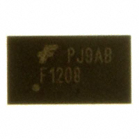
FSA1208BQX
F1208
-40 to +85°C
Package
20-Lead, Quad, Molded Leadless Package
(MLP), 2.5 x 4.5 mm
DIMM
1A
2A
3A
4A
5A
6A
7A
8A
FSA1208
OE
VCC
1B
2B
3B
4B
5B
6B
7B
8B
DIMM
DIMM Slot
Figure 1. Analog Sym bol
© 2008 Semiconductor Components Industries, LLC
October-2017, Rev. 2
Publication Order Number:
FSA1208/D
FSA1208 — Low-Power, Eight-Port, High-Speed Isolation Switch
FSA1208
Low-Power, Eight-Port, High-Speed Isolation Switch
�19
18
17
16
15
14
13
B1
12
20
11
1
10
2
3
4
5
6
7
8
B2
B3
B4
B5
B6
B7
B8
/OE
NC
VCC
GND
A1
9
A2
A3
A4
A5
A6
Figure 2. Pin Assignm ents for MLP (Top Through View )
Pin Definitions
Pin #
Name
Description
20
/OE
Sw itch Enable
2-9
A1-A8
A Side of Bus
12-19
B8-B1
B Side of Bus
11
NC
No Connection
1
VCC
Pow er
10
GND
Ground
Truth Table
/OE
Function
HIGH
Disconnect
LOW
A1-A8=B1-B8
www.onsemi.com
2
A7
A8
FSA1208 — Low-Power, Eight-Port, High-Speed Isolation Switch
Pin Configurations
�Stresses exceeding the absolute maximum ratings may damage the device. The device may not function or be
operable above the recommended operating conditions and stressing the parts to these levels is not recommended.
In addition, extended exposure to stresses above the recommended operating conditions may affect device reliability.
The absolute maximum ratings are stress ratings only.
Symbol
V CC
Parameter
Supply Voltage
V CNTRL
DC Input Voltage (/OE)
(1)
(1)
V SW
DC Sw itch I/O Voltage
IIK
DC Input Diode Current
IOUT
DC Output Current
TSTG
Storage Temperature
Min.
Max.
Unit
-0.50
+5.25
V
-0.50
V CC
V
-0.50
5.25
-50
-65
All Pins
Human Body Model, JEDEC: JESD22-A114
ESD
V
mA
50
mA
+150
°C
7.5
I/O to GND
8
Pow er to GND
16
Charged Device Model, JEDEC: JESD22-C101
kV
2
Note:
1. The input and output negative ratings may be exceeded if the input and output diode current ratings are
observed.
Recommended Operating Conditions
The Recommended Operating Conditions table defines the conditions for actual device operation. Recommended
operating conditions are specified to ensure optimal performance to the datasheet specifications. ON Semiconductor
does not recommend exceeding them or designing to Absolute Maximum Ratings.
Symbol
V CC
TA
Max.
Unit
2.3
4.3
V
0
V CC
V
Sw itch I/O Voltage
-0.5
V CC
V
Operating Temperature
-40
+85
°C
Supply Voltage
(2)
V CNTRL
V SW
Parameter
Control Input Voltage (S, /OE)
Note:
2. The control input must be held HIGH or LOW; it must not float.
www.onsemi.com
3
Min.
FSA1208 — Low-Power, Eight-Port, High-Speed Isolation Switch
Absolute Maximum Ratings
�All typical values are at 25°C unless otherw ise specified.
Symbol
Parameter
Conditions
VCC (V)
Min. Typ. Max.
Clamp Diode Voltage
V IH
Input Voltage High
V IL
Input Voltage Low
IIN
Control Input Leakage
V SW=0 to V CC
4.3
IOZ
Off State Leakage
0 A, B 3.6 V
4.3
V SW=0 V, ION=-10 mA
Figure 3
2.5
7
V SW=1.8 V, ION=-10 mA
Figure 3
2.5
15
Sw itch On Resistance
(3)
2.5
-1.2
Units
V IK
RON
IIN=-18 mA
TA=- 40ºC to +85ºC
V
2.3 to 3.6
1.3
V
4.3
1.7
V
2.3 to 3.6
0.5
V
4.3
0.7
V
-1
1
µA
-2
2
µA
ICC
Quiescent Supply Current
V IN=0 or V CC, IOUT=0
4.3
1
µA
ICCT
Increase in ICC Current Per
Control Voltage and V CC
V IN=1.8 V
2.7
10
µA
Note:
3. Measured by the voltage drop betw een A and B pins at the indicated current through the sw itch.
On resistance is determined by the low er of the voltage on the tw o (A or B ports).
AC Electrical Characteristics
All typical values are for V CC=2.5 V at 25°C unless otherw ise specified.
Symbol
Parameter
Conditions
VCC (V)
TA=- 40ºC to +85ºC
Min.
Typ.
Max.
Units
ton
Turn-On Time, /OE to Output
RL=50 Ω, CL=5 pF
V SW=1.8 V
Figure 4, Figure 5
2.3 to 3.6
15
34
ns
tuff
Turn-Off Time, /OE to Output
RL=50 Ω, CL=5 pF
V SW=1.8 V
Figure 4, Figure 5
2.3 to 3.6
12
25
ns
tad
Propagation Delay
RL=50 Ω, CL=5 pF
Figure 4, Figure 6
3.3
0.35
ns
(4)
OIRR
Off Isolation
RL=50 Ω, f=400 MHz
Figure 11
2.3 to 3.6
-40
dB
Xtalk
Non-Adjacent Channel
Crosstalk
RL=50 Ω, f=100 MHz
Figure 12
2.3 to 3.6
-40
dB
1000
MHz
750
MHz
BW
-3dB Bandw idth
RL=50 Ω, CL=0 pF
Figure 10
RL=50 Ω, CL=5 pF
Figure 10
Note:
4. Guaranteed by characterization.
www.onsemi.com
4
2.3 to 3.6
FSA1208 — Low-Power, Eight-Port, High-Speed Isolation Switch
DC Electrical Characteristics
�Symbol
Parameter
Conditions
(5)
tSK(O)
Channel-to-Channel Skew
tSK(P)
Skew of Opposite Transitions
(5)
of the Same Output
tSK(PKG)
Package-to-Package Skew
(5)
VCC (V)
TA=- 40ºC to +85ºC
Min. Typ. Max.
Units
CL=5 pF
3.3
40
80
ps
CL=5 pF
3.3
15
40
ps
CL=5 pF
3.3
60
100
ps
Note:
5. Guaranteed by characterization.
Capacitance
Symbol
Parameter
Conditions
TA=- 40ºC to +85ºC
Min.
Typ. Max.
CIN
Control Pin Input Capacitance
V CC=0.2 V, f=1 MHz
2.0
CON
D+/D- On Capacitance
V CC=2.5 V, /OE=0 V, f=1 MHz
Figure 9
6.0
COFF
D1n, D2n Off Capacitance
V CC and /OE=2.5 V, f=1 MHz
Figure 8
2.5
www.onsemi.com
5
Units
pF
FSA1208 — Low-Power, Eight-Port, High-Speed Isolation Switch
High-Speed-Related AC Electrical Characteristics
�VON
An
Bn
VSW
GND
ION
/O
E
GND
V Se l= 0
r Vc c
= O / ION
o
N
V
Figure 3. On Resistance
RO
N
An
tRISE = 2.5ns
Bn
VSW
CL
GN D RS
RL
tFALL = 2.5ns
VCC
V OUT
Input – V/OE , VSel
GN D
10%
GND
V Sel
90%
90%
VCC /2
VCC /2
10%
VOH
90%
GND
90%
Output- VOUT
RL , RS , and C L are func tion s of the appl ica tion
e nvi ron ment ( s ee AC tabl es for spec ifi c val ues).
CL i ncl udes test fix tur e and s tr ay c apac ita nce.
Figure 4. AC Test Circuit Load
VOL
tON
tOFF
Figure 5. Turn-On / Turn-Off Waveform s
tRISE = 500ps
tFALL = 500ps
+400mV
90%
0V
- 400mV
10%
90%
10%
Output
t PHL
Figure 6. Propagation Delay
(t ry t o – 500ps)
Figure 7. Intra-Pair Skew Test tSK(P)
An
Capacitance
Meter
/OE
Capacitance
Meter
t PLH
An
/OE
VS el = 0 o r Vc c
B
n
V Sel = 0 or Vcc
Bn
Figure 8. Channel Off Capacitance
Figure 9. Channel On Capacitance
www.onsemi.com
6
FSA1208 — Low-Power, Eight-Port, High-Speed Isolation Switch
Test Diagrams
�(Continued)
Network Analyzer
RS
V IN
VS
GND
GND
VSel
GND
VOUT
GND
RT
GND
RS and RT are functions of the application
environment (see AC Tables for specific values).
Figure 10. Bandw idth
Ne two rk Ana lyz r
e
RS
VSel
V IN
GN D
RT
VS
GND
GND
V OUT
GND
GND
RT
RS and RT a r functions of the app lication
enviro nmen te (see A C tab les fo r sp ecific Values).
GND
Off isolation = 20 Log (VOUT/ V IN )
Figure 11. Channel Off Isolation
Networ k An alyz r
e
R
N
C
S
GND
V IN
VS
GND
VSel
GND
RT
GND
GND
RS and RT ar functio ns o f the ap plication e nviro nment
(see AC tabele s for speci fi c valu es).
RT
VOUT
GND
Crosstalk = 20 L og (V OUT / VIN )
Figure 12. Non-Adjacent Channel-to-Channel Crosstalk
www.onsemi.com
7
FSA1208 — Low-Power, Eight-Port, High-Speed Isolation Switch
Test Diagrams
�FSA1208 — Low-Power, Eight-Port, High-Speed Isolation Switch
Physical Dimensions
Figure 13. 20-Lead, Molded Leadless Package (MLP)
www.onsemi.com
8
�FSA1208 — Low-Power, Eight-Port, High-Speed Isolation Switch
ON Semiconductor and the ON Semiconductor logo are trademarks of Semiconductor Components Industries, LLC dba ON Semiconductor or its subsidiaries in the
United States and/or other countries. ON Semiconductor owns the rights to a number of patents, trademarks, copyrights, trade secrets, and other intellectual property. A
listing of ON Semiconductor’s product/patent coverage may be accessed at www.onsemi.com/site/pdf/Patent-Marking.pdf. ON Semiconductor reserves the right to make
changes without further notice to any products herein. ON Semiconductor makes no warranty, representation or guarantee regarding the suitability of its products for any
particular purpose, nor does ON Semiconductor assume any liability arising out of the application or use of any product or circuit, and specifically disclaims any and all
liability, including without limitation special, consequential or incidental damages. Buyer is responsible for its products and applications using ON Semiconductor
products, including compliance with all laws, regulations and safety requirements or standards, regardless of any support or applications information provided by
ON Semiconductor. “Typical” parameters which may be provided in ON Semiconductor data sheets and/or specifications can and do vary in different applications and
actual performance may vary over time. All operating parameters, including “Typicals” must be validated for each customer application by customer’s technical experts.
ON Semiconductor does not convey any license under its patent rights nor the rights of others. ON Semiconductor products are not designed, intended, or authorized for
use as a critical component in life support systems or any FDA Class 3 medical devices or medical devices with a same or similar classification in a foreign jurisdiction or
any devices intended for implantation in the human body. Should Buyer purchase or use ON Semiconductor products for any such unintended or unauthorized
application, Buyer shall indemnify and hold ON Semiconductor and its officers, employees, subsidiaries, affiliates, and distributors harmless against all claims, costs,
damages, and expenses, and reasonable attorney fees arising out of, directly or indirectly, any claim of personal injury or death associated with such unintended or
unauthorized use, even if such claim alleges that ON Semiconductor was negligent regarding the design or manufacture of the part. ON Semiconductor is an Equal
Opportunity/Affirmative Action Employer. This literature is subject to all applicable copyright laws and is not for resale in any manner.
PUBLICATION ORDERING INFORMATION
LITERATURE FULFILLMENT:
Literature Distribution Center for ON Semiconductor
19521 E. 32nd Pkwy, Aurora, Colorado 80011 USA
Phone: 303-675-2175 or 800-344-3860 Toll Free USA/Canada
Fax : 303-675-2176 or 800-344-3867 Toll Free USA/Canada
Email: orderlit@onsemi.com
N. Amer ican Technical Support: 800-282-9855 Toll Free
USA/Canada.
Eur ope, Middle East and Afr ica Technical Support:
Phone: 421 33 790 2910
Japan Customer Focus Center
Phone: 81-3-5817-1050
www.onsemi.com
9
ON Semiconductor Website: www.onsemi.com
Or der Literature: http://www.onsemi.com/orderlit
For additional information, please contact your local
Sales Representative
�


 工商网监
湘ICP备2023018690号
工商网监
湘ICP备2023018690号
