Is Now Part of
To learn more about ON Semiconductor, please visit our website at
www.onsemi.com
Please note: As part of the Fairchild Semiconductor integration, some of the Fairchild orderable part numbers
will need to change in order to meet ON Semiconductor’s system requirements. Since the ON Semiconductor
product management systems do not have the ability to manage part nomenclature that utilizes an underscore
(_), the underscore (_) in the Fairchild part numbers will be changed to a dash (-). This document may contain
device numbers with an underscore (_). Please check the ON Semiconductor website to verify the updated
device numbers. The most current and up-to-date ordering information can be found at www.onsemi.com. Please
email any questions regarding the system integration to Fairchild_questions@onsemi.com.
ON Semiconductor and the ON Semiconductor logo are trademarks of Semiconductor Components Industries, LLC dba ON Semiconductor or its subsidiaries in the United States and/or other countries. ON Semiconductor owns the rights to a number
of patents, trademarks, copyrights, trade secrets, and other intellectual property. A listing of ON Semiconductor’s product/patent coverage may be accessed at www.onsemi.com/site/pdf/Patent-Marking.pdf. ON Semiconductor reserves the right
to make changes without further notice to any products herein. ON Semiconductor makes no warranty, representation or guarantee regarding the suitability of its products for any particular purpose, nor does ON Semiconductor assume any liability
arising out of the application or use of any product or circuit, and specifically disclaims any and all liability, including without limitation special, consequential or incidental damages. Buyer is responsible for its products and applications using ON
Semiconductor products, including compliance with all laws, regulations and safety requirements or standards, regardless of any support or applications information provided by ON Semiconductor. “Typical” parameters which may be provided in ON
Semiconductor data sheets and/or specifications can and do vary in different applications and actual performance may vary over time. All operating parameters, including “Typicals” must be validated for each customer application by customer’s
technical experts. ON Semiconductor does not convey any license under its patent rights nor the rights of others. ON Semiconductor products are not designed, intended, or authorized for use as a critical component in life support systems or any FDA
Class 3 medical devices or medical devices with a same or similar classification in a foreign jurisdiction or any devices intended for implantation in the human body. Should Buyer purchase or use ON Semiconductor products for any such unintended
or unauthorized application, Buyer shall indemnify and hold ON Semiconductor and its officers, employees, subsidiaries, affiliates, and distributors harmless against all claims, costs, damages, and expenses, and reasonable attorney fees arising out
of, directly or indirectly, any claim of personal injury or death associated with such unintended or unauthorized use, even if such claim alleges that ON Semiconductor was negligent regarding the design or manufacture of the part. ON Semiconductor
is an Equal Opportunity/Affirmative Action Employer. This literature is subject to all applicable copyright laws and is not for resale in any manner.
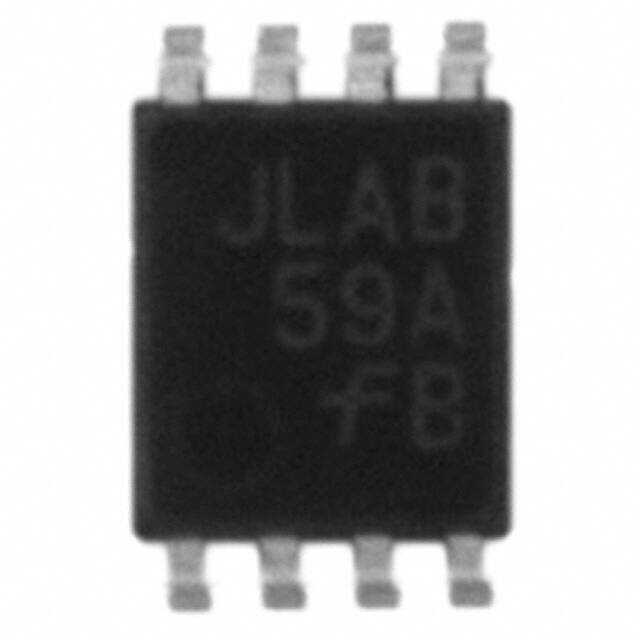
�FSA1259A
Low-Voltage, 1 Ω Dual SPST Analog Switch with
Power-Off Isolation
Features
Description
The FSA1259A is a high-performance, dual, Single-Pole
/ Single-Throw (SPST) analog switch. The device
features ultra-low RON of 1 at 4.5 V VCC and operates
over the wide VCC range of 1.65 V to 5.50 V.
Power-Off Isolation (VCC=0 V)
1 Ω On Resistance (RON) for 4.5V VCC
0.25 Ω Maximum RON Flatness for 4.5 V VCC
Space-Saving, US8 Surface Mount Package
Broad VCC Operating Range: 1.65 V to 5.50 V
Fast Turn-On and Turn-Off Times
Break-Before-Make Enable Circuitry
The FS1259A allows for reduced input thresholds on the
select pins.
The device is fabricated with sub-micron CMOS
technology to achieve fast switching speeds and is
designed for break-before-make operation.
Applications
Cellular Phone
Portable Media Player
PDA
Ordering Information
Part Number
Top
Mark
Operating
Temperature Range
Package
Packing
Method
FSA1259AK8X
59A
-40°C to +85°C
8-Lead US8, JEDEC MO-187, Variation
CA, 3.0 mm Wide
3000 Units
Tape and Reel
1A
1
8
V CC
1B
2
7
1S
2S
3
6
2B
GND
4
5
2A
Figure 1.
© 2007 Fairchild Semiconductor Corporation
FSA1259A Rev. 1.0.8
Analog Symbols
www.fairchildsemi.com
FSA1259A — Low-Voltage, 1 Dual SPST Analog Switch with Power-Off Isolation
April 2014
�1A
1
8
Vcc
1B
2S
2
7
1S
3
6
GND
4
5
2B
2A
Figure 2.
Pin Assignments (Top View)
Pin Definitions
Pin #
Name
Description
1
1A
Data Port
2
1B
Data Port
3
2S
Control Input
4
GND
5
2A
Data Port
6
2B
Data Port
7
1S
Control Input
8
VCC
Supply Voltage
Ground
Truth Table
Control Input (S)
Function
LOW
Disconnected
HIGH
A Connected to B
© 2007 Fairchild Semiconductor Corporation
FSA1259A Rev. 1.0.8
FSA1259A — Low-Voltage, 1 SPST Analog Switch with Power-Off Isolation
Pin Assignments
www.fairchildsemi.com
2
�Stresses exceeding the absolute maximum ratings may damage the device. The device may not function or be
operable above the recommended operating conditions and stressing the parts to these levels is not recommended.
In addition, extended exposure to stresses above the recommended operating conditions may affect device reliability.
The absolute maximum ratings are stress ratings only.
Symbol
VCC
Parameter
Supply Voltage
(1)
Min.
Max.
Unit
-0.5
7.0
V
VCC +-0.5
V
VSW
Switch Voltage
-0.5
VIN
(1)
Input Voltage
-0.5
6.5
V
IIK
Input Diode Current
-50
mA
ISW
Switch Current (Continuous)
200
mA
Peak Switch Current (Pulsed at 1 ms Duration,
很抱歉,暂时无法提供与“FSA1259AK8X”相匹配的价格&库存,您可以联系我们找货
免费人工找货