DATA SHEET
www.onsemi.com
Low-Power, Dual SIM Card
Analog Switch
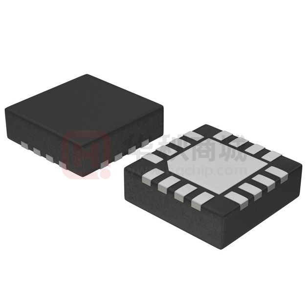
WQFN16 3x3, 0.5P
CASE 510BS
FSA2567
Description
The FSA2567 is a bi−directional, low−power, dual double−pole,
double−throw (4PDT) analog switch targeted at dual SIM card
multiplexing. It is optimized for switching the WLAN−SIM data and
control signals and dedicates one channel as a supply−source switch.
The FSA2567 is compatible with the requirements of SIM cards and
features a low on capacitance (CON) of 10 pF to ensure high−speed
data transfer. The VSIM switch path has a low RON characteristic to
ensure minimal voltage drop in the dual SIM card supply paths.
The FSA2567 contains special circuitry that minimizes current
consumption when the control voltage applied to the SEL pin is lower
than the supply voltage (VCC). This feature is especially valuable in
ultra−portable applications, such as cell phones; allowing direct
interface with the general−purpose I/Os of the baseband processor.
Other applications include switching and connector sharing in
portable cell phones, PDAs, digital cameras, printers, and notebook
computers.
Features
•
•
•
•
•
•
•
•
Low On Capacitance for Data Path: 10 pF Typical
Low On Resistance for Data Path: 6 W Typical
Low On Resistance for Supply Path: 0.4 W Typical
Wide VCC Operating Range: 1.65 V to 4.3 V
Low Power Consumption: 1 mA Maximum
♦ 15 mA Maximum ICCT Over Expanded Voltage Range
(VIN = 1.8 V, VCC = 4.3 V)
Wide −3 db Bandwidth: >160 MHz
Packaged in:
♦ Pb−free 16−Lead MLP & 16−Lead UMLP
3 kV ESD Rating, >12 kV Power/GND ESD Rating
UQFN16 1.8x2.6, 0.4P
CASE 523BF
MARKING DIAGRAM
$Y&Z&2&K
FSA
2567
GX, FSA2567
$Y
&Z
&2
&K
GX&K
&2&Z
= Device Code
= onsemi Logo
= Assembly Plant Code
= 2−Digit Date Code
= 2−Digits Lot Run Traceability Code
ORDERING INFORMATION
See detailed ordering and shipping information on page 2 of
this data sheet.
Applications
• Cell Phone, PDA, Digital Camera, and Notebook
• LCD Monitor, TV, and Set−Top Box
© Semiconductor Components Industries, LLC, 2008
November, 2021 − Rev. 3
1
Publication Order Number:
FSA2567/D
�FSA2567
ORDERING INFORMATION
Top Mark
Operating
Temperature Range
FSA2567MPX
FSA2567
−40 to +85°C
FSA2567UMX
GX
Part Number
Package
Shipping†
16−Lead, Molded Leadless Package (MLP)
Quad, JEDEC MO−220, 3 mm Square
3000 / Tape & Reel
16−Lead, Quad, Ultrathin Molded Leadless
Package (UMLP), 1.8 x 2.6 mm
5000 / Tape & Reel
†For information on tape and reel specifications, including part orientation and tape sizes, please refer to our Tape and Reel Packaging
Specifications Brochure, BRD8011/D.
1VSIM
VSIM
2VSIM
1RST
RST
2RST
1CLK
CLK
2CLK
1DAT
DAT
2DAT
Sel
Figure 1. Analog Symbol
1
12 DAT
Sel
2
11 2DAT
2RST
3
10
RST
4
9
5
6
7
8
1RST
GND
2CLK
CLK
(Not connected to GND)
1CLK
Figure 2. Pad Assignment MLP16
(Top Through View)
12
DAT
Sel
2
11
2DAT
2RST
3
10
No Connect
RST
4
9
1CLK
Description
nVSIM
Multiplexed SIM Supply Inputs
VSIM, DAT, RST, CLK
Sel
5
6
7
8
Figure 3. Pad Assignment UMLP16
(Top Through View)
Pin No.
Multiplexed Data Source Inputs
1DAT
1
PIN DESCRIPTION
nDAT, nRST, nCLK
VCC
1VSIM
CLK
1VSIM
14 13
2CLK
13
2VSIM
1DAT
14
15
GND
VCC
15
VSIM
2V SIM
16
16
1RST
V SIM
PIN ASSIGNMENTS
Common SIM Ports
Switch Select
www.onsemi.com
2
�FSA2567
TRUTH TABLE
Sel
Function
Logic LOW
1DAT = DAT, 1RST = RST, 1CLK = CLK, 1VSIM = VSIM
Logic HIGH
2DAT = DAT, 2RST = RST, 2CLK = CLK, 2VSIM = VSIM
ABSOLUTE MAXIMUM RATINGS
Symbol
Min
Max
Unit
Supply Voltage
−0.5
+5.5
V
VCNTRL
DC Input Voltage (Sel) (Note 1)
−0.5
VCC
V
VSW
DC Switch I/O Voltage (Note 1)
−0.5
VCC + 0.3
V
DC Input Diode Current
−50
−
mA
−
350
mA
VCC
IIK
Parameter
ISIM
DC Output Current − VSIM
IOUT
DC Output Current – DAT, CLK, RST
TSTG
Storage Temperature
ESD
Human Body Model, JEDEC: JESD22−A114
−
35
mA
−65
+150
°C
All Pins
−
3
kV
I/O to GND
−
12
−
2
Charged Device Model, JEDEC: JESD22−C101
Stresses exceeding those listed in the Maximum Ratings table may damage the device. If any of these limits are exceeded, device functionality
should not be assumed, damage may occur and reliability may be affected.
1. The input and output negative ratings may be exceeded if the input and output diode current ratings are observed.
RECOMMENDED OPERATING CONDITIONS
Symbol
VCC
VCNTRL
Parameter
Supply Voltage
Control Input Voltage (Sel) (Note 2)
Min
Max
Unit
1.65
4.30
V
0
VCC
V
−0.5
VCC
V
VSW
Switch I/O Voltage
ISIM
DC Output Current − VSIM
−
150
mA
IOUT
DC Output Current – DAT, CLK, RST
−
25
mA
−40
+85
°C
TA
Operating Temperature
Functional operation above the stresses listed in the Recommended Operating Ranges is not implied. Extended exposure to stresses beyond
the Recommended Operating Ranges limits may affect device reliability.
2. The control input must be held HIGH or LOW; it must not float.
www.onsemi.com
3
�FSA2567
DC ELECTRICAL CHARACTERISTICS (All typical values are at 25°C, 3.3 V VCC unless otherwise specified.)
TA = −40°C to 85°C
Symbol
Parameter
VIK
Clamp Diode Voltage
VIH
Input Voltage High
VIL
IIN
Conditions
IIN = −18 mA
Input Voltage Low
VCC (V)
Min
Typ
Max
Unit
2.7
−
−
−1.2
V
1.65 to 2.3
1.1
−
−
V
2.7 to 3.6
1.3
−
−
4.3
1.7
−
−
1.65 to 2.3
−
−
0.4
2.7 to 3.6
−
−
0.5
4.3
−
−
0.7
V
Control Input Leakage
VSW = 0 to VCC
4.3
−1
−
1
mA
Inc(off),
Ino(off)
Off State Leakage
nRST, nDAT, nCLK, nVSIM = 0.3 V
or 3.6 V
Figure 10
4.3
−60
−
60
nA
ROND
Data Path Switch On Resistance
(Note 3)
VSW = 0, 1.8 V, ION = −20 mA
Figure 9
1.8
−
7.0
12.0
W
VSW = 0, 2.3 V, ION = −20 mA
Figure 9
2.7
−
6.0
10.0
VSW = 0, 1.8 V, ION = −100 mA
Figure 9
1.8
−
0.5
0.7
VSW = 0, 2.3 V, ION = −100 mA
Figure 9
2.7
−
0.4
0.6
Data Path Delta On Resistance
(Note 4)
VSW = 0 V, ION = −20 mA
2.7
−
0.2
−
W
ICC
Quiescent Supply Current
VCNTRL = 0 or VCC, IOUT = 0
4.3
−
−
1.0
mA
ICCT
Increase in ICC Current Per Control
Voltage and VCC
VCNTRL = 2.6 V, VCC = 4.3 V
4.3
−
5.0
10.0
mA
VCNTRL = 1.8 V, VCC = 4.3 V
4.3
−
7.0
15.0
mA
RONV
DROND
VSIM Switch On Resistance
(Note 3)
W
3. Measured by the voltage drop between nDAT, nRST, nCLK and relative common port pins at the indicated current through the switch.
On resistance is determined by the lower of the voltage on the relative ports.
4. Guaranteed by characterization.
www.onsemi.com
4
�FSA2567
AC ELECTRICAL CHARACTERISTICS (All typical values are for VCC = 3.3 V at 25°C unless otherwise specified.)
TA = −40°C to 85°C
Symbol
tOND
Parameter
Conditions
VCC (V)
Min
Typ
Max
Unit
Turn−On Time Sel to Output
(DAT, CLK, RST)
RL = 50 W, CL = 35 pF
VSW = 1.5 V
Figure 11, Figure 12
1.8 (Note 5)
−
65
95
ns
2.7 to 3.6
−
42
60
ns
Turn−Off Time Sel to Output
(DAT, CLK, RST)
RL = 50 W, CL = 35 pF
VSW = 1.5 V
Figure 11, Figure 12
1.8 (Note 5)
−
30
50
ns
2.7 to 3.6
−
20
40
ns
Turn−On Time
Sel to Output (VSIM)
RL = 50 W, CL = 35 pF
VSW = 1.5 V
Figure 11, Figure 12
1.8 (Note 5)
−
55
80
ns
2.7 to 3.6
−
35
55
ns
Turn−Off Time
Sel to Output (VSIM)
RL = 50 W, CL = 35 pF
VSW = 1.5 V
Figure 11, Figure 12
1.8 (Note 5)
−
35
50
2.7 to 3.6
−
22
40
ns
Propagation Delay (Note 5)
(DAT, CLK, RST)
CL = 35 pF, RL = 50 W
Figure 11, Figure 13
3.3
−
0.25
−
ns
tBBMD
Break−Before−Make (Note 5)
(DAT, CLK, RST)
RL = 50 W, CL = 35 pF
VSW1 = VSW2 = 1.5 V
Figure 15
2.7 to 3.6
3
18
−
ns
tBBMV
Break−Before−Make (Note 5)
(VSIM)
RL = 50 W, CL = 35 pF
VSW1 = VSW2 = 1.5 V
Figure 15
2.7 to 3.6
3
12
−
ns
Charge Injection (DAT, CLK, RST)
CL = 50 pF, RGEN = 0 W,
VGEN = 0 V
2.7 to 3.6
−
10
−
pC
OIRR
Off Isolation (DAT, CLK, RST)
RL = 50 W, f = 10 MHz
Figure 17
2.7 to 3.6
−
−60
−
dB
Xtalk
Non−Adjacent Channel Crosstalk
(DAT, CLK, RST)
RL = 50 W, f = 10 MHz
Figure 18
2.7 to 3.6
−
−60
−
dB
BW
−3 db Bandwidth (DAT, CLK, RST)
RL = 50 W, CL = 5 pF
Figure 16
2.7 to 3.6
−
475
−
MHz
tOFFD
tONV
tOFFV
tPD
Q
5. Guaranteed by characterization.
CAPACITANCE
TA = −40°C to 85°C
Symbol
CIN
Parameter
Conditions
Min
Typ
Max
Unit
pF
Control Pin Input Capacitance
VCC = 0 V
−
1.5
−
COND
RST, CLK, DAT On Capacitance (Note 6)
VCC = 3.3 V, f = 1 MHz, Figure 20
−
10
12
CONV
VSIM On Capacitance (Note 6)
VCC = 3.3 V, f = 1 MHz, Figure 20
−
110
150
COFFD
RST, CLK, DAT Off Capacitance
VCC = 3.3 V, Figure 19
−
3
−
COFFV
VSIM Off Capacitance
VCC = 3.3 V, Figure 19
−
40
−
6. Guaranteed by characterization.
www.onsemi.com
5
�FSA2567
TYPICAL PERFORMANCE CHARACTERISTICS
5.00
4.00
RON (Ohms)
6.00
0.50
85°C
25°C
−40°C
3.00
0.00
1.00
2.00
85°C
0.40
25°C
0.30
−40°C
0.20
0.10
0.00
−1.00
3.00
0.00
VIN, VCC = 2.7 V
1.00
VIN, VCC = 2.7 V
Figure 4. RON Data Path
Figure 5. RON VSIM
Frequency Response
0
1
10
100
Frequency Response
1
10
100
Off Isolation (dB)
−10
−30
−50
−70
−90
−110
Frequency (MHz)
VCC = 2.7 V
Figure 6. Off Isolation
0
Cross Talk (dB)
2.00
−1.00
−5
−15
−25
−35
−45
−55
−65
−75
−85
−95
−105
−115
−125
Frequency (MHz)
VCC = 2.7 V
Figure 7. Crosstalk
Gain (dB)
RON (Ohms)
7.00
0
−1
−2
−3
−4
−5
−6
−7
−8
1
10
Frequency Response
100
Frequency (MHz)
CL = 5 pF, VCC = 2.7 V
Figure 8. Bandwidth
www.onsemi.com
6
1000
10000
2.00
3.00
�FSA2567
TEST DIAGRAMS
VON
nVSIM, nRST,
nCLK, or nDAT
NC
VSIM, RST,
CLK, or DAT
I nA(OFF)
A
VSW
VSW
I ON
GND
GND
RON = VON / ION
GND
VSel = 0 or VCC
VSel = 0 or VCC
Figure 9. On Resistance
Figure 10. Off Leakage
tRISE = 2.5 ns
nVSIM, nRST,
nCLK, or nDAT
VCC
VSIM, RST,
CLK, or DAT
CL
GND
VOUT
RL
90%
VCC / 2
10%
GND
VOH
GND
Sel
90%
Input − VSel
VSW
tFALL = 2.5 ns
VCC / 2
10%
90%
90%
Output − VOUT
RL and CL are functions of the application
environment (see tables for specific values).
CL includes test fixture and stray capacitance.
VOL
Figure 11. AC Test Circuit Load
t OFF
Figure 12. Turn−On / Turn−Off Waveforms
tRISE = 2.5 ns
tFALL = 2.5 ns
90%
Input − VSW
90%
VCC / 2
10 %
GND
t ON
VCC / 2
10%
VOH
Output − VOUT
50%
50%
VOL
t pLH
t pHL
Figure 13. Propagation Delay
VCC
nVSIM, nRST,
nCLK, or nDAT
Logic Input
VSIM, RST,
CLK, or DAT
CL
Sel
On
Off
DVOUT
VSW
GND
Off
0V
RL
VOUT
GND
VOUT
Q = DVOUT · CL
Figure 14. Charge Injection
www.onsemi.com
7
�FSA2567
TEST DIAGRAMS (Continued)
nVSIM, nRST,
nCLK, or nDAT
VSW1
GND
tRISE = 2.5 ns
VSIM, RST,
CLK, or DAT
CL
VSW2
GND
GND
RL
VCC
90%
VCC / 2
Input − VSel
VOUT
10%
0V
VOUT
0.9 · VOUT
Sel
0.9 · VOUT
tBBM
RL and CL are functions of the application
environment (see tables for specific values).
CL includes test fixture and stray capacitance.
Figure 15. Break−Before−Make Interval Timing
Network Analyzer
RS
VIN
GND
Network Analyzer
RS
VS
GND
VSEL
GND
GND
RT
RS and RT are functions of the application
environment (see tables for specific values).
GND
RT
VSel
VOUT
VIN
GND
VOUT
GND
GND
GND
RT
RS and RT are functions of the application
environment (see tables for specific values).
GND
VS
GND
Off isolation = 20 Log (VOUT / VIN)
Figure 16. Bandwidth
Figure 17. Channel Off Isolation
Network Analyzer
RS
NC
GND
VIN
VS
GND
VSel
GND
RT
GND
GND
RT
RS and RT are functions of the application
environment (see tables for specific values).
VOUT
GND
Crosstalk = 20 Log (VOUT / VIN)
Figure 18. Non−Adjacent Channel−to−Channel Crosstalk
VSIM, RST,
CLK, or DAT
nVSIM, nRST,
nCLK, or nDAT
Capacitance
Meter
Capacitance
Meter
VSel = 0 or VCC
f = 1 MHz
f = 1 MHz
nVSIM, nRST,
nCLK, or nDAT
VSel = 0 or VCC
nVSIM, nRST,
nCLK, or nDAT
Figure 19. Channel Off Capacitance
Figure 20. Channel On Capacitance
www.onsemi.com
8
�MECHANICAL CASE OUTLINE
PACKAGE DIMENSIONS
WQFN16 3x3, 0.5P
CASE 510BS
ISSUE O
DOCUMENT NUMBER:
DESCRIPTION:
98AON13630G
WQFN16 3X3, 0.5P
DATE 31 AUG 2016
Electronic versions are uncontrolled except when accessed directly from the Document Repository.
Printed versions are uncontrolled except when stamped “CONTROLLED COPY” in red.
PAGE 1 OF 1
ON Semiconductor and
are trademarks of Semiconductor Components Industries, LLC dba ON Semiconductor or its subsidiaries in the United States and/or other countries.
ON Semiconductor reserves the right to make changes without further notice to any products herein. ON Semiconductor makes no warranty, representation or guarantee regarding
the suitability of its products for any particular purpose, nor does ON Semiconductor assume any liability arising out of the application or use of any product or circuit, and specifically
disclaims any and all liability, including without limitation special, consequential or incidental damages. ON Semiconductor does not convey any license under its patent rights nor the
rights of others.
© Semiconductor Components Industries, LLC, 2019
www.onsemi.com
�MECHANICAL CASE OUTLINE
PACKAGE DIMENSIONS
UQFN16 1.8x2.6, 0.4P
CASE 523BF
ISSUE O
DOCUMENT NUMBER:
DESCRIPTION:
98AON13709G
UQFN16 1.8x2.6, 0.4P
DATE 31 OCT 2016
Electronic versions are uncontrolled except when accessed directly from the Document Repository.
Printed versions are uncontrolled except when stamped “CONTROLLED COPY” in red.
PAGE 1 OF 1
ON Semiconductor and
are trademarks of Semiconductor Components Industries, LLC dba ON Semiconductor or its subsidiaries in the United States and/or other countries.
ON Semiconductor reserves the right to make changes without further notice to any products herein. ON Semiconductor makes no warranty, representation or guarantee regarding
the suitability of its products for any particular purpose, nor does ON Semiconductor assume any liability arising out of the application or use of any product or circuit, and specifically
disclaims any and all liability, including without limitation special, consequential or incidental damages. ON Semiconductor does not convey any license under its patent rights nor the
rights of others.
© Semiconductor Components Industries, LLC, 2019
www.onsemi.com
�onsemi,
, and other names, marks, and brands are registered and/or common law trademarks of Semiconductor Components Industries, LLC dba “onsemi” or its affiliates
and/or subsidiaries in the United States and/or other countries. onsemi owns the rights to a number of patents, trademarks, copyrights, trade secrets, and other intellectual property.
A listing of onsemi’s product/patent coverage may be accessed at www.onsemi.com/site/pdf/Patent−Marking.pdf. onsemi reserves the right to make changes at any time to any
products or information herein, without notice. The information herein is provided “as−is” and onsemi makes no warranty, representation or guarantee regarding the accuracy of the
information, product features, availability, functionality, or suitability of its products for any particular purpose, nor does onsemi assume any liability arising out of the application or use
of any product or circuit, and specifically disclaims any and all liability, including without limitation special, consequential or incidental damages. Buyer is responsible for its products
and applications using onsemi products, including compliance with all laws, regulations and safety requirements or standards, regardless of any support or applications information
provided by onsemi. “Typical” parameters which may be provided in onsemi data sheets and/or specifications can and do vary in different applications and actual performance may
vary over time. All operating parameters, including “Typicals” must be validated for each customer application by customer’s technical experts. onsemi does not convey any license
under any of its intellectual property rights nor the rights of others. onsemi products are not designed, intended, or authorized for use as a critical component in life support systems
or any FDA Class 3 medical devices or medical devices with a same or similar classification in a foreign jurisdiction or any devices intended for implantation in the human body. Should
Buyer purchase or use onsemi products for any such unintended or unauthorized application, Buyer shall indemnify and hold onsemi and its officers, employees, subsidiaries, affiliates,
and distributors harmless against all claims, costs, damages, and expenses, and reasonable attorney fees arising out of, directly or indirectly, any claim of personal injury or death
associated with such unintended or unauthorized use, even if such claim alleges that onsemi was negligent regarding the design or manufacture of the part. onsemi is an Equal
Opportunity/Affirmative Action Employer. This literature is subject to all applicable copyright laws and is not for resale in any manner.
ADDITIONAL INFORMATION
TECHNICAL PUBLICATIONS:
Technical Library: www.onsemi.com/design/resources/technical−documentation
onsemi Website: www.onsemi.com
ONLINE SUPPORT: www.onsemi.com/support
For additional information, please contact your local Sales Representative at
www.onsemi.com/support/sales
�


 工商网监
湘ICP备2023018690号
工商网监
湘ICP备2023018690号
