ON Semiconductor
Is Now
To learn more about onsemi™, please visit our website at
www.onsemi.com
onsemi and and other names, marks, and brands are registered and/or common law trademarks of Semiconductor Components Industries, LLC dba “onsemi” or its affiliates and/or
subsidiaries in the United States and/or other countries. onsemi owns the rights to a number of patents, trademarks, copyrights, trade secrets, and other intellectual property. A listing of onsemi
product/patent coverage may be accessed at www.onsemi.com/site/pdf/Patent-Marking.pdf. onsemi reserves the right to make changes at any time to any products or information herein, without
notice. The information herein is provided “as-is” and onsemi makes no warranty, representation or guarantee regarding the accuracy of the information, product features, availability, functionality,
or suitability of its products for any particular purpose, nor does onsemi assume any liability arising out of the application or use of any product or circuit, and specifically disclaims any and all
liability, including without limitation special, consequential or incidental damages. Buyer is responsible for its products and applications using onsemi products, including compliance with all laws,
regulations and safety requirements or standards, regardless of any support or applications information provided by onsemi. “Typical” parameters which may be provided in onsemi data sheets and/
or specifications can and do vary in different applications and actual performance may vary over time. All operating parameters, including “Typicals” must be validated for each customer application
by customer’s technical experts. onsemi does not convey any license under any of its intellectual property rights nor the rights of others. onsemi products are not designed, intended, or authorized
for use as a critical component in life support systems or any FDA Class 3 medical devices or medical devices with a same or similar classification in a foreign jurisdiction or any devices intended for
implantation in the human body. Should Buyer purchase or use onsemi products for any such unintended or unauthorized application, Buyer shall indemnify and hold onsemi and its officers, employees,
subsidiaries, affiliates, and distributors harmless against all claims, costs, damages, and expenses, and reasonable attorney fees arising out of, directly or indirectly, any claim of personal injury or death
associated with such unintended or unauthorized use, even if such claim alleges that onsemi was negligent regarding the design or manufacture of the part. onsemi is an Equal Opportunity/Affirmative
Action Employer. This literature is subject to all applicable copyright laws and is not for resale in any manner. Other names and brands may be claimed as the property of others.
�Features
Description
The FSA3051 is a 6 Ω, bi-directional, low -pow er, tw oport, high-speed, Single Pole / Double Throw (SPDT)
analog sw itch. It features an extremely low on
capacitance (CON) of 7.7 pF and w ide bandw idth of
1.0 GHz.
Low On Capacitance: 7.7 pF Typical
Low On Resistance: 6 Ω Typical
Low Pow er Consumption: 1 μA Maximum
- 15 μA Maximum
ICCT over an Expanded Voltage
Range (V IN=1.8 V, V CC=5.5 V)
The FSA3051 contains special circuitry on the sw itch
I/O pins for applications w here the V CC supply is
pow ered-off (V CC=0 V), w hich allow s the device to
w ithstand an over-voltage condition. This device is
designed to minimize current consumption even w hen
the control voltage applied to the select (S) pin is low er
than the supply voltage (V CC). This feature is especially
valuable to ultra-portable applications, such as cell
phones, allow ing for direct interface w ith the generalpurpose I/Os of the baseband processor. Other
applications include sw itching in portable cell phones,
PDAs, digital cameras, printers, and notebook
computers.
Wide -3 db Bandw idth: 1.0 GHz
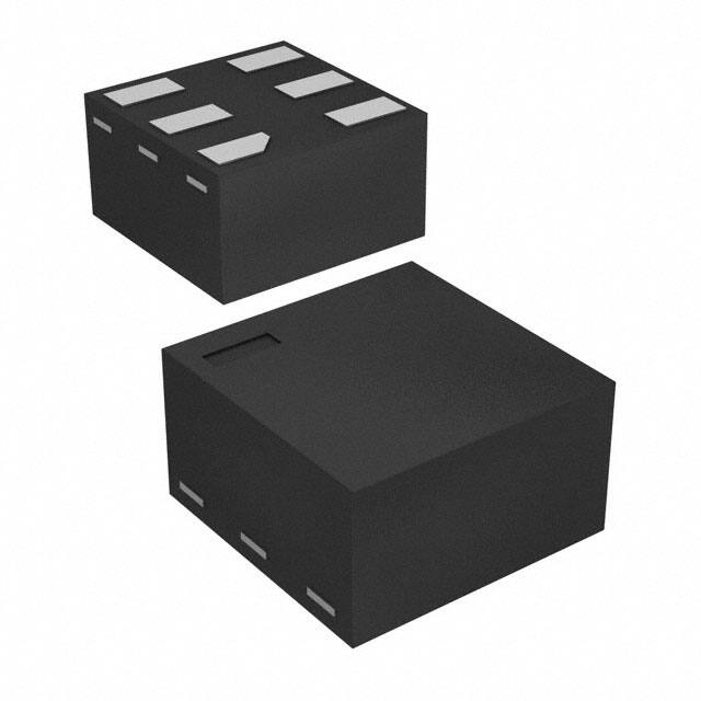
Packaged in Ultra Small 6-Lead TMLP
Broad V CC Operating Range: 1.6 V to 5.5 V
Over-Voltage Tolerance (OVT) on all Data Ports
up to 6 V w ithout External Components
Applications
Cell Phone, PDA, Digital Camera, and Notebook
LCD Monitor, TV, and Set-Top Box
Ordering Information
Part Number
Top
Mark
Operating
Temperature
Range
FSA3051TMX
NT
-40 to +85°C
6-Lead, Dual, Ultra-ultrathin Molded Leadless Package
(TMLP), 1.0 x 1.0 mm. Top left unit orientation in carrier tape.
FSA3051TMX-F147
NT
-40 to +85°C
6-Lead, Dual, Ultra-ultrathin Molded Leadless Package
(TMLP), 1.0 x 1.0 mm. Bottom left unit orientation in carrier
tape.
Package
MicroPak™ is a trademark of ON Semiconductor Corporation.
© 2014 Semiconductor Components Industries, LLC.
October-2017, Rev.2
Publication Order Number:
FSA3051/D
FSA3051 — High Performance SPDT Analog Switch with Over Voltage Tolerance
FSA3051 —High Performance SPDT Analog Switch
with Over-Voltage Tolerance
�Figure 1.
Logic Sym bol
Figure 2.
Pin Assignments
Figure 3.
6-Lead TMLP (Top-Through View )
Pin Definitions
UMLP Pin#
Name
Description
1
B1
2
GND
3
B0
Data Port
4
A
Data Port
5
V CC
6
S
Data Port
Ground
Supply Voltage
Sw itch Select
Truth Table
S
Function
LOW
B0 connected to A
HIGH
B1 connected to A
Notes:
1. LOW ≤V IL.
2. HIGH ≥V IH.
www.onsemi.com
2
Analog Sym bol
FSA3051 — High Performance SPDT Analog Switch with Over Voltage Tolerance
Analog Symbols
�Stresses exceeding the absolute maximum ratings may damage the device. The device may not function or be
operable above the recommended operating conditions and stressing the parts to these levels is not recommended.
In addition, extended exposure to stresses above the recommended operating conditions may affect device reliability.
The absolute maximum ratings are stress ratings only.
Symbol
V CC
V CNTRL
Parameter
Supply Voltage
(3)
DC Input Voltage
(3)
Min.
Max.
Unit
-0.5
6.0
V
-0.5
V CC
V
6.00
V
V SW
DC Sw itch I/O Voltage
-0.50
IIK
DC Input Diode Current
-50
IOUT
DC Output Current
TSTG
Storage Temperature
MSL
Moisture Sensitivity Level (JEDEC J-STD-020A)
-65
Human Body Model, ANSI/ESDA/JEDEC
ESD
JS-001-2012
All Pins
2
I/O to GND
2
Pow er to GND
2
Charged Device Model, JEDEC: JESD22-C101
mA
50
mA
+150
°C
1
Level
kV
1
Note:
3. The input and output negative ratings may be exceeded if the input and output diode current ratings are observed.
Recommended Operating Conditions
The Recommended Operating Conditions table defines the conditions for actual device operation. Recommended
operating conditions are specified to ensure optimal performance to the datasheet specifications. ON Semiconductor
does not recommend exceeding them or designing to Absolute Maximum Ratings.
Symbol
V CC
V CNTRL
V SW
TA
Parameter
Min.
Max.
Unit
1.6
5.5
V
0
V CC
V
Sw itch I/O Voltage
-0.5
5.5
V
Operating Temperature
-40
+85
°C
Supply Voltage
Control Input Voltage (S)
(4)
Note:
4. The control input must be held HIGH or LOW and it must not float.
www.onsemi.com
3
FSA3051 — High Performance SPDT Analog Switch with Over Voltage Tolerance
Absolute Maximum Ratings
�All typical value are at TA=25°C unless otherw ise specified.
Symbol
Parameter
V IK
Clamp Diode Voltage
V IH
Input Voltage High
V IL
Input Voltage Low
IIN
Control Input Leakage
IOZ
IOFF
RON
RON
Condition
IIN=-18 mA
Off State Leakage
Pow er-Off Leakage Current
(All I/O Ports)
(5)
VCC (V)
TA=- 40°C to +85°C
Min. Typ.
Max.
3.0
-1.2
1.8 to 4.3
1.3
4.3 to 5.5
1.7
1.8 to 4.3
0.5
4.3 to 5.5
0.7
-1
1
5.5
-1
1
V SW=0 V to V CC
1.8
-2
2
V SW=0 V to 3.6 V
5.5
-2
2
0
-2
2
V SW=0 V to 4.3 V, V CC=0 V
Figure 5
V SW=0.4 V, ION=-8 mA
Figure 4
3.0
4
10
V SW=1.8 V, ION=-8 mA
Figure 4
3.0
6
10
V SW=0.4 V, ION=-8 mA
Figure 4
1.8
6
10
V SW=1.8 V, ION=-8 mA
Figure 4
1.8
14
25
3.0
35
1.8
40
V SW=0.4 V, ION = -8 mA
ICC
Quiescent Supply Current
V CNTRL=0 or V CC, IOUT=0
5.5
1
V CNTRL=1.8 V
3.0
10
ICCT
Increase in ICC Current per
Control Voltage and V CC
V CNTRL=2.6 V
5.5
10
V CNTRL=1.8 V
5.5
15
Notes:
5. Measured by the voltage drop betw een A and Bn pins at the indicated current through the sw itch.
On resistance is determined by the low er of the voltage on the tw o (A or Bn ports).
6. ΔRON = RON maximum - RON minimum measured at identical V CC, temperature, and voltage levels.
7. Guaranteed by characterization.
www.onsemi.com
4
µA
µA
µA
Ω
Sw itch On Resistance
On Resistance Match
(5,6)
Betw een Channels
ΔRON
V
Ω
Sw itch On Resistance
(5)
V
V
1.8
V CNTRL=0 to V CC
Unit
mΩ
µA
µA
FSA3051 — High Performance SPDT Analog Switch with Over Voltage Tolerance
DC Electrical Characteristics
�All typical value are for V CC=3.3 V at TA=25°C unless otherw ise specified.
Symbol
Parameter
Condition
VCC (V)
TA=- 40°C to +85°C
Min.
Typ.
tON
Turn-On Time
S to Output
RL=50 Ω, CL=5 pF, V SW=0.8 V,
Figure 6, Figure 7
3.0 to 3.6
34
1.8
110
tOFF
Turn-Off Time
S to Output
RL=50 Ω, CL=5 pF, V SW=0.8 V,
Figure 6, Figure 7
3.0 to 3.6
23
1.8
50
tPD
Propagation Delay
CL=5 pF, RL=50 Ω, Figure 6,
Figure 8
3.3
0.2
1.8
0.3
tBBM
Break-Before-Make
RL=50 Ω, CL=5 pF,
V SW1=V SW2=0.8 V, Figure 9
OIRR
Off Isolation
RL=50 Ω, f=240 MHz, Figure 11
Xtalk
Crosstalk
RL=50 Ω, f=240 MHz, Figure 12
RL=50 Ω, CL=0 pF, V SW=0.4 V
BW
-3 db Bandw idth
RL=50 Ω, CL=0 pF, Figure 10
RL=50 Ω, CL=5 pF, Figure 10
3.0 to 3.6
15
Max.
ns
ns
ns
50
1.8
100
1.8
-20
3.0 to 3.6
-23
Unit
ns
dB
1.8
-18
dB
3.0 to 3.6
-23
dB
1.8
810
MHz
1
GHz
750
MHz
3.0 to 3.6
Note:
8. Guaranteed by characterization. Not production tested.
Capacitance
(9)
TA=- 40°C to +85°C
Symbol
CIN
CON
COFF
Parameter
Condition
Control Pin Input
Capacitance
A Port On Capacitance
Bn Port Off Capacitance
VCC (V)
Min.
Typ.
0
1.5
f=1 MHz,
3.0
7.7
f=240 MHz, Figure 14
3.3
7.7
f=1 MHz,
1.8
10.0
f=240 MHz, Figure 14
1.8
5.0
f=1 MHz
3.0
3.3
f=240 MHz, Figure 13
3.3
3.3
f=1 MHz
1.8
5.0
f=240 MHz, Figure 13
1.8
4.0
Note:
9. Not production tested.
www.onsemi.com
5
Max.
Unit
pF
FSA3051 — High Performance SPDT Analog Switch with Over Voltage Tolerance
AC Electrical Characteristics(8)
�VON
IA
NC
(OFF)
A
VSW
Bn
S e lect
A
GN D
VSW
GND
Se lect
RON =
VON / ION
Figure 4.
Bn
VS
VS
ION
=0 orVcc
**Each switch port is teste d sep a rate ly
GN D
= 0or Vcc
On Resistance
Figure 5.
Off Leakage
tR I SE = 2.5ns
tF A LL = 2.5n s
A
VCC
VSW
CL
GN D RS
RL
VOUT
90%
Inp ut – Vs
10 %
GN D
GND
90%
VC C /2
VC C /2
10%
VO H
VS
90%
Ou tpu t- VO UT
90%
GND
VO L
tO N
RL , RS , and C L are func tio ns o f the app lic ati on
e nvi ro nment ( s ee A C Ta bles for sp eci fic values)
CL i ncl udes tes t fix tur e and str ay cap aci tanc e.
Figure 6.
AC Test Circuit Load
Figure 7.
Turn-On / Turn-Off Waveform s
400mV
50%
Input
50%
0V
tPLH
tPHL
VOH
Output
50%
50%
VOL
Figure 8.
Propagation Delay (t Rt F – 500 ps)
www.onsemi.com
6
tO F F
FSA3051 — High Performance SPDT Analog Switch with Over Voltage Tolerance
Test Diagrams
�(Continued)
t RI S E = 2. 5ns
Vcc
Bn
A
VS W 1
GND
RL
VOU T
GND
GND
10%
0V
VOUT
CL
VS W 2
90%
Vcc/2
Input - VS
0.9*Vou t
0.9*Vou t
RS
tBB M
VS
R L , RS , and C L are f unc tion s of the applic at ion
env iron men t (s ee AC Tab les f or s pec if ic values)
C L includ es t est fix tu re and st ray c apac it anc e.
GND
Figure 9.
Break-Before-Make Interval Tim ing
Netw ork Analyzer
Net work Analyzer
RS
RS
V IN
VS
GND
VS
GND
RT
R S and RT are func tions of the applicat ion
environm ent (see AC Tables for s pecif ic values).
Figure 10.
VS
GN D
VOU T
G ND
RS and R T are functions of the application
environment (see AC Tables for specif ic values).
GND
V IN
G ND
G ND
VOU T
GND
GN D
RT
VS
GND
RT
GN D
Of f isolation = 20 Log (V
OUT / VIN)
Bandw idth
Figure 11.
Channel Off Isolation
Net work Analyzer
RS
VIN
GND
VS
VS
GND
GND
RT
GND
GND
RT
RS and R T are f unc tions of the application environment
(see AC Tables for specif ic values).
VOUT
GND
Crosstalk = 20 Log (VOUT / VI )
Figure 12.
Capacitance
Meter
Channel-to-Channel Crosstalk
Capacitance
Meter
Bn
Bn
S=LOW or HIGH
S=LOW or HIGH
A
A
Figure 13.
Channel Off Capacitance
Figure 14.
www.onsemi.com
7
Channel On Capacitance
FSA3051 — High Performance SPDT Analog Switch with Over Voltage Tolerance
Test Diagrams
�Figure 15.
TMLP Carrier Tape Packing
Part Number
Unit Orientation
FSA3051TMX
Top Left
FSA3051TMX-F147
Bottom Left
www.onsemi.com
8
FSA3051 — High Performance SPDT Analog Switch with Over Voltage Tolerance
Carrier Tape Orientation
�0.89
0.70
0.05 C
1.00±0.050
2X
6
5
B
A
0.35
4
6X 0.40
PIN 1
MIN 250uM
1.00±0.050
1
2
0.66
1.06
0.05 C
3
TOP VIEW
2X
6X 0.20
RECOMMENDED LAND PATTERN
0.05 C
C
0.370±0.030
SIDE VIEW
6X
(0.05) 4X
1
DETAIL A
2
3
0.20±0.025
(0.05) 6X
45°
CHAMFER
DETAIL A
PIN 1 LEAD SCALE: 2X
(0.30)
6X
0.30±0.025
6
5
4
0.35
0.60
NOTES:
A. NO JEDEC STANDARD APPLIES
B. DIMENSIONS ARE IN MILLIMETERS.
C. DIMENSIONS AND TOLERANCES PER ASME Y14.5M, 2009
D. LANDPATTERN RECOMMENDATION IS BASED ON FSC
DESIGN.
E. DRAWING FILENAME AND REVISION: MKT-TMLP06AREV2
BOTTOM VIEW
0.05
C B A
0.05 C
6-Lead, Dual, Ultra-ultrathin Molded Leadless Package (TMLP), 1.0 x 1.0 m m
www.onsemi.com
9
FSA3051 — High Performance SPDT Analog Switch with Over Voltage Tolerance
Physical Dimensions
�PUBLICATION ORDERING INFORMATION
LITERATURE FULFILLMENT:
Literature Distribution Center for ON Semiconductor
19521 E. 32nd Pkwy, Aurora, Colorado 80011 USA
Phone: 303-675-2175 or 800-344-3860 Toll Free USA/Canada
Fax : 303-675-2176 or 800-344-3867 Toll Free USA/Canada
Email: orderlit@onsemi.com
N. Amer ican Technical Support: 800-282-9855 Toll Free
USA/Canada.
Eur ope, Middle East and Afr ica Technical Support:
Phone: 421 33 790 2910
Japan Customer Focus Center
Phone: 81-3-5817-1050
www.onsemi.com
10
ON Semiconductor Website: www.onsemi.com
Or der Literature: http://www.onsemi.com/orderlit
For additional information, please contact your local
Sales Representative
FSA3051 — High Performance SPDT Analog Switch with Over Voltage Tolerance
ON Semiconductor and the ON Semiconductor logo are trademarks of Semiconductor Components Industries, LLC dba ON Semiconductor or its subsidiaries in the
United States and/or other countries. ON Semiconductor owns the rights to a number of patents, trademarks, copyrights, trade secrets, and other intellectual property. A
listing of ON Semiconductor’s product/patent coverage may be accessed at www.onsemi.com/site/pdf/Patent-Marking.pdf. ON Semiconductor reserves the right to make
changes without further notice to any products herein. ON Semiconductor makes no warranty, representation or guarantee regarding the suitability of its products for any
particular purpose, nor does ON Semiconductor assume any liability arising out of the application or use of any product or circuit, and specifically disclaims any and all
liability, including without limitation special, consequential or incidental damages. Buyer is responsible for its products and applications using ON Semiconductor
products, including compliance with all laws, regulations and safety requirements or standards, regardless of any support or applications information provided by
ON Semiconductor. “Typical” parameters which may be provided in ON Semiconductor data sheets and/or specifications can and do vary in different applications and
actual performance may vary over time. All operating parameters, including “Typicals” must be validated for each customer application by customer’s technical experts.
ON Semiconductor does not convey any license under its patent rights nor the rights of others. ON Semiconductor products are not designed, intended, or authorized for
use as a critical component in life support systems or any FDA Class 3 medical devices or medical devices with a same or similar classification in a foreign jurisdiction or
any devices intended for implantation in the human body. Should Buyer purchase or use ON Semiconductor products for any such unintended or unauthorized
application, Buyer shall indemnify and hold ON Semiconductor and its officers, employees, subsidiaries, affiliates, and distributors harmless against all claims, costs,
damages, and expenses, and reasonable attorney fees arising out of, directly or indirectly, any claim of personal injury or death associated with such unintended or
unauthorized use, even if such claim alleges that ON Semiconductor was negligent regarding the design or manufacture of the part. ON Semiconductor is an Equal
Opportunity/Affirmative Action Employer. This literature is subject to all applicable copyright laws and is not for resale in any manner.
�