Features
Description
The FSA642 is a bi-directional, low -pow er, high-speed
analog sw itch. The pin out is designed to ease
differential signal layout and is configured as a triplepole, double-throw sw itch (TPDT). The FSA642 is
optimized for sw itching betw een tw o MIPI devices, such
as cameras or LCD displays and on-board Multimedia
Application Processors (MAP).
Low On Capacitance: 7.0 pF Typical
Low On Resistance: 7.0 Ω Typical
Wide -3db Bandw idth: 1 GHz Typical
24-Lead UMLP (2.5 x 3.4 mm) Package
8 kV ESD Rating; >16 kV Pow er/GND ESD Rating
Applications
Dual Camera Applications for Cell Phones
Dual LCD Applications for Cell Phones,
Digital Camera Displays, and View finders
The FSA642 is compatible w ith the requirements of
Mobile Industry Processor Interface (MIPI). The low capacitance design allow s the FSA642 to sw itch signals
that exceed 500 MHz in frequency. Superior channel-tochannel crosstalk immunity minimizes interference and
allow s the transmission of high-speed differential signals
and single-ended signals, as described by the MIPI
specification.
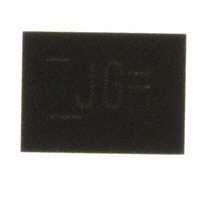
Ordering Information
Part Number Top Mark Operating Temperature Range
FSA642UMX
JG
-40 to +85°C
Camera 1
D
Camera 2
C
D D
C
FSA642
D
Package
24-Lead, Quad, Ultrathin Molded Leadless
Package (UMLP), 2.5 x 3.4 mm
LCD 1
LCD 2
C
D
C
FSA642
C
D
MAP Processor
D D
C
MAP Processor
Figure 1. Application Block Diagram
© 2008 Semiconductor Components Industries, LLC.
December-2017, Rev. 2
Publication Order Number:
FSA642/D
FSA642 — Low-Power, Three-Port, High-Speed MIPI Switch
FSA642
Low-Power, Three-Port, High-Speed MIPI Switch
�15
14
13
CLKAN
DA1P
DA1N
DA2P
20
16
CLKAP
DB2P
17
DB2N
19
18
DA2N
12
DB1P
SEL
11
21
DB1N
VCC
10
22
CLKBP
GND
9
23
CLKBN
/OE
8
24
NC
NC
7
CLKP
CLKN
D1P
D1N
D2P
D2N
642
1
2
3
4
5
6
Figure 2. Pin Configuration (Top Through View )
Pin Definitions
Pin #
Name
1, 2
CLKP, CLKN
Clock Path (Common)
Description
3, 4
D1P, D1N
Data Path 1 (Common)
Data Path 2 (Common)
5, 6
D2P, D2N
7, 24
NC
No Connect (Float)
8
/OE
Output Enable (Active Low )
9
GND
Ground
10
VCC
Pow er
11
SEL
Select (0=A, 1=B)
12, 13
DA2N, DA2P
Data Path (A2)
14, 15
DA1N, DA1P
Data Path (A1)
16, 17
CLKAN, CLKAP
Clock Path (A)
18, 19
DB2N, DB2P
Data Path (2B)
20, 21
DB1P, DB1N
Data Path (1B)
22, 23
CLKBP, CLKBN,
Clock Path (B)
www.onsemi.com
2
FSA642 — Low-Power, Three-Port, High-Speed MIPI Switch
Pin Configuration
�FSA642
CLKAP (17)
CLKAN (16)
(1) CLKP
(2) CLKN
DA1P (15)
DA1N (14)
DA2P (13)
DA2N (12)
(3) D1P
(4) D1N
CLKBP (22)
CLKBN (23)
DB1P (20)
DB1N (21)
(5) D2P
(6) D2N
DB2P (19)
DB2N (18)
(8) /OE
(11) SEL
Sw itch
Control
(10) V CC
(9) GND
Figure 3. Functional Diagram
Truth Table
SEL
/OE
Function
Don’t Care
HIGH
Disconnect
LOW
LOW
D1, D2, CLK=DA1, DA2, CLKA
HIGH
LOW
D1, D2, CLK=DB1, DB2, CLKB
www.onsemi.com
3
FSA642 — Low-Power, Three-Port, High-Speed MIPI Switch
Functional Diagram
�Stresses exceeding the absolute maximum ratings may damage the device. The device may not function or be
operable above the recommended operating conditions and stressing the parts to these lev els is not recommended.
In addition, extended exposure to stresses above the recommended operating conditions may affect device reliability.
The absolute maximum ratings are stress ratings only.
Symbol
V CC
V CNTRL
Parameter
Supply Voltage
DC Input Voltage (SEL, /OE)
(1)
V SW
DC Sw itch I/O Voltage
IIK
DC Input Diode Current
IOUT
DC Output Current
TSTG
Storage Temperature
ESD
(1)
Min.
Max.
Unit
-0.50
+5.25
V
-0.5
V CC
V
-0.5
V CC + 0.3
V
-50
-65
Human Body Model, JEDEC: JESD22-A114
mA
50
mA
+150
°C
All Pins
6.5
I/O to GND
8.0
Pow er to GND
16.0
Charged Device Model, JEDEC: JESD22-C101
kV
2.5
Note:
1. The input and output negative ratings may be exceeded if the input and output diode current ratings are observed.
Recommended Operating Conditions
The Recommended Operating Conditions table defines the conditions for actual device operation. Recommended
operating conditions are specified to ensure optimal performance to the datasheet specifications. ON Semiconductor
does not recommend exceeding them or designing to Absolute Maximum Ratings.
Symbol
V CC
V CNTRL
V SW
TA
Parameter
Min.
Max.
Unit
2.65
4.30
V
0
V CC
V
Sw itch I/O Voltage
-0.5
V CC-1
V
Operating Temperature
-40
+85
°C
Supply Voltage
Control Input Voltage (SEL, /OE)
(2)
Note:
2. The control input must be held HIGH or LOW; it must not float.
www.onsemi.com
4
FSA642 — Low-Power, Three-Port, High-Speed MIPI Switch
Absolute Maximum Ratings
�All typical values are TA=25°C unless otherw ise specified.
Symbol
Parameter
Conditions
TA=-40 to +85ºC
VCC (V)
V IK
Clamp Diode Voltage
IIN=-18 mA
IIN
Control Input Leakage
V SW=0 to 4.3 V
V IH
Input Voltage High
V IN=0 to V CC
V IL
Input Voltage Low
V IN=0 to V CC
IOZ
Off-State Leakage
A,B=0+0.3 V to V CC-0.3
4.3
ICC
Quiescent Supply Current
V CNTRL=0 or V CC, IOUT=0
ICCT
Increase in ICC Current Per
Control Voltage and V CC
V CNTRL=1.8 V
Min.
Typ. Max.
2.775
4.3
-1
2.650 to 2.775
1.3
4.3
1.7
Units
-1.2
V
1
µA
V
2.650 to 2.775
0.5
V
2
µA
4.3
1.0
µA
2.775
1.5
µA
-2
DC Electrical Characteristics, Low-Speed Mode
All typical values are TA=25°C unless otherw ise specified.
Symbol
RON
∆RON
Parameter
LS Sw itch On Resistance
LS Delta RON
Conditions
(3)
(4)
VCC (V)
TA=-40 to +85ºC
Min. Typ. Max.
V SW=1.2 V, ION=-10 mA, Figure 4
2.65
10
V SW=1.2 V, ION=-10 mA (Intra-pair)
2.65
0.65
14
Units
Notes:
3. Measured by the voltage drop betw een A/B and CLK/Dn pins at the indicated current through the sw itch.
4. Guaranteed by characterization.
DC Electrical Characteristics, High-Speed Mode
All typical values are TA=25°C unless otherw ise specified.
Symbol
RON
∆RON
Parameter
HS Sw itch On Resistance
HS Delta RON
(6)
Conditions
(5)
VCC (V)
TA=-40 to +85ºC
V SW=0.4 V, ION=-10 mA, Figure 4
2.65
7.0
V SW=0.4 V, ION=-10 mA (Intra-pair)
2.65
0.65
9.5
Notes:
5. Measured by the voltage drop betw een A, B, and Dn pins at the indicated current through the sw itch.
6. Guaranteed by characterization.
www.onsemi.com
5
Units
Min. Typ. Max.
FSA642 — Low-Power, Three-Port, High-Speed MIPI Switch
DC Electrical Characteristics
�All values are at RL=50Ω and RS=50Ω and all typical values are V CC=2.775V at TA=25°C unless otherw ise specified.
Symbol
Parameter
Conditions
(7)
OIRR
Off Isolation
Xtalk
Non-Adjacent Channel
(7)
Crosstalk
BW
-3 db Bandw idth
tON
Turn-On Time
SEL, /OE to Output
tOFF
Turn-Off Time
SEL, /OE to Output
tPD
Propagation Delay
tBBM
Break-Before-Make Time
(7)
(7)
VCC (V)
TA=-40ºC to +85ºC
Min.
Typ.
Max.
Units
f=100 MHz, RT=50 Ω
Figure 14
2.775
-35
dB
f=100 MHz, RT=50 Ω
Figure 15
2.775
-55
dB
CL=0 pF, RT=50 Ω
Figure 13
2.775
1.0
GHz
CL=5 pF, V SW=1.2 V
Figure 6, Figure 7
2.650 to 2.775
20
37
ns
CL=5 pF, V SW=1.2 V
Figure 6, Figure 7
2.650 to 2.775
15
27
ns
CL=5 pF
Figure 6, Figure 8
2.775
0.25
CL=5 pF,
V SW1=V SW2=1.2 V
Figure 12
2.650 to 2.775
3
5
ns
8
ns
Note:
7. Guaranteed by characterization.
AC Electrical Characteristics, High-Speed
All typical values are V CC=2.775V at TA=25°C unless otherw ise specified.
Symbol
Parameter
Conditions
TA=-40ºC to +85ºC
Min.
Typ.
Max.
Units
tSK(Part_Part)
Channel-to-Channel Skew
(8,9)
Across Multiple Parts
V SW=0.2 Vdiff PP, CL=5 pF
40
80
ps
tSK(Chl_Chl)
Channel-to-Channel Skew Within V SW=0.2 Vdiff PP, CL=5 pF,
(8)
a Single Part
Figure 9
15
30
ps
Skew of Opposite Transitions in
(8)
the Same Differential Channel
10
20
ps
tSK(Pulse)
V SW=0.2 Vdiff PP, CL=5 pF
Notes:
8. Guaranteed by characterization.
9. Assumes the same V CC and temperature for all devices.
Capacitance
Symbol
Parameter
Conditions
CIN
Control Pin Input
(10)
Capacitance
CON
Dn/CLK- On Capacitance
COFF
Dn/CLK Off Capacitance
TA=-40ºC to +85ºC
Min.
V CC=0 V
(10)
(10)
V CC=2.775 V, /OE=0 V, f=1 MHz,
at 25°C, Figure 11
V CC=2.775 V , /OE=2.775 V,
f=1 MHz, Figure 10
Note:
10. Guaranteed by characterization.
www.onsemi.com
6
Typ.
Max.
Units
1.5
6.0
7.0
2.5
9.0
pF
FSA642 — Low-Power, Three-Port, High-Speed MIPI Switch
AC Electrical Characteristics
�VON
I Dn(OFF)
NC
A
DA/Bn
VSW
Dn
VSW
Select
GND
I ON
Select
RON =
VON / ION
V Sel =
GND
V Sel =
GND
0 orV
V cc
0 orV cc
**Each switch port is tested separately
Figure 4. On Resistance
Figure 5. Off Leakage
tRISE = 2.5ns
DA B
/ n
tFALL = 2.5ns
Dn
VSW
CL
GND RS
RL
VOUT
VCC
Input – V/OE , VSel
GND
10%
GND
VSel
90%
90%
VCC /2
VCC /2
10%
VOH
GN D
90%
90%
Output- VOUT
R L , RS, an C L ar f u c tions o f th a p lic ation
env ironmednt (s e e ACn Ta bles forespe pific v lues)
c ac itaanc e .
C L inc lu es tes tefix ture an s t ra cap
d
d
y
.
VOL
tON
tOFF
Figure 6. AC Test Circuit Load
Figure 7. Turn-On / Turn-Off Waveform s
Figure 8. Propagation Delay (t Rt F – 500 ps)
Figure 9. Channel-to-Channel Skew
DA/Bn
S
Capacitance
Meter
Capacitance DA/Bn
Meter
VSEL =0 or VCC
S
VSEL =0 or VCC
DA/Bn
DA/Bn
Figure 10. Channel Off Capacitance
Figure 11. Channel On Capacitance
www.onsemi.com
7
FSA642 — Low-Power, Three-Port, High-Speed MIPI Switch
Test Diagrams
�(Continued)
tRI SE= 2.5ns
Vcc
HSDn
Dn
VSW1
GND
1 %
0
0V
VOUT
CL
VSW2
RL
V OUT
GND
GND
9 %
V0
cc/ 2
I nput - VSe l
0.9*Vo
RS
0. 9*Vo
t
u
u
VSel
tBBM
RL , RS , and C L ar functio ns o f the application
envir onme nt (seee A C Tab les fo r sp ecific v l ues).
CL includes test fixture a nd str a ca pacitaan ce.
y
GND
Figure 12. Break-Before-Make Interval Tim ing
Network Analyzer
RS
V IN
VS
GND
GND
VSel
GND
VOUT
GND
RT
GND
RS and RT are functions of the application
environment (see AC Tables for specific values).
Figure 13. Bandw idth
Network Analyzer
RS
VSel
V IN
GND
RT
VS
GND
GND
V OUT
GND
GND
RT
RS and RT are functions of the application
environment (see AC Tables for specific values).
GND
Off isolation = 20 Log (V OUT / VIN)
Figure 14. Channel Off Isolation
Network Analyzer
NC
RS
GND
V IN
VS
VSel
GND
GND
RT
GND
GND
RS and RT are functions of the application environment
(see AC Tables for specific values).
RT
V OUT
GND
Crosstalk = 20 Log (VOUT / VIN)
Figure 15. Non-Adjacent Channel-to-Channel Crosstalk
www.onsemi.com
8
t
FSA642 — Low-Power, Three-Port, High-Speed MIPI Switch
Test Diagrams
�FSA642 — Low-Power, Three-Port, High-Speed MIPI Switch
Physical Dimensions
Figure 16.
24-Lead UMLP Package
Product-Specific Dimensions
Description
Nominal Values (mm)
Description
Nominal Values (mm)
Overall Height
PKG Standoff
Lead Thickness
Lead Width (24x)
0.500
0.026
0.152
0.200
Lead Length (23x)
Lead Length, Pin 1 (1x)
Lead Pitch
Body Length (X)
Body Width (Y)
0.4
0.5
0.4
3.4
2.5
www.onsemi.com
9
�FSA642 — Low-Power, Three-Port, High-Speed MIPI Switch
Figure 17. Tape and Reel Packing Specification, page 1
www.onsemi.com
10
�FSA642 — Low-Power, Three-Port, High-Speed MIPI Switch
Figure 18. Tape and Reel Packing Specification, page 2
www.onsemi.com
11
�FSA642 — Low-Power, Three-Port, High-Speed MIPI Switch
ON Semiconductor and the ON Semiconductor logo are trademarks of Semiconductor Components Industries, LLC dba ON Semiconductor or its subsidiaries in the
United States and/or other countries. ON Semiconductor owns the rights to a number of patents, trademarks, copyrights, trade secrets, and other intellectual property. A
listing of ON Semiconductor’s product/patent coverage may be accessed at www.onsemi.com/site/pdf/Patent-Marking.pdf. ON Semiconductor reserves the right to make
changes without further notice to any products herein. ON Semiconductor makes no warranty, representation or guarantee regarding the suitability of its products for any
particular purpose, nor does ON Semiconductor assume any liability arising out of the application or use of any product or ci rcuit, and specifically disclaims any and all
liability, including without limitation special, consequential or incidental damages. Buyer is responsible for its products and applications using ON Semiconductor
products, including compliance with all laws, regulations and safety requirements or standards, regardless of any support or applications information provided by
ON Semiconductor. “Typical” parameters which may be provided in ON Semiconductor data sheets and/or specifications can and do vary in different applications and
actual performance may vary over time. All operating parameters, including “Typicals” must be validated for each customer application by customer’s technical experts.
ON Semiconductor does not convey any license under its patent rights nor the rights of others. ON Semiconductor products are not designed, intended, or authorized for
use as a critical component in life support systems or any FDA Class 3 medical devices or medical devices with a same or simi lar classification in a foreign jurisdiction or
any devices intended for implantation in the human body. Should Buyer purchase or use ON Semiconductor products for any such unintended or unauthorized
application, Buyer shall indemnify and hold ON Semiconductor and its officers, employees, subsidiaries, affiliates, and distr ibutors harmless against all claims, costs,
damages, and expenses, and reasonable attorney fees arising out of, directly or indirectly, any claim of personal injury or death associated with such unintended or
unauthorized use, even if such claim alleges that ON Semiconductor was negligent regarding the design or manufacture of the part. ON Semiconductor is an Equal
Opportunity/Affirmative Action Employer. This literature is subject to all applicable copyright laws and is not for resale in any manner.
PUBLICATION ORDERING INFORMATION
LITERATURE FULFILLMENT:
Literature Distribution Center for ON Semiconductor
19521 E. 32nd Pkwy, Aurora, Colorado 80011 USA
Phone: 303-675-2175 or 800-344-3860 Toll Free USA/Canada
Fax : 303-675-2176 or 800-344-3867 Toll Free USA/Canada
Email: orderlit@onsemi.com
N. Amer ican Technical Support: 800-282-9855 Toll Free
USA/Canada.
Eur ope, Middle East and Afr ica Technical Support:
Phone: 421 33 790 2910
Japan Customer Focus Center
Phone: 81-3-5817-1050
www.onsemi.com
12
ON Semiconductor Website: www.onsemi.com
Or der Literature: http://www.onsemi.com/orderlit
For additional information, please contact your local
Sales Representative
�


 工商网监
湘ICP备2023018690号
工商网监
湘ICP备2023018690号