FSA9480 — USB 2.0 Accessory Switch
Features
Description
The FSA9480 is a USB port accessory detector and
2
switch. The FSA9480 is fully controlled using I C™ and
enables USB data, stereo and mono audio, video,
microphone, and UART data to use a common
connector port. It is designed for compatibility with CEA936-A car kit adapters, USB 2.0 signaling, and USB
OTG (on-the-go). The architecture is designed to allow
audio signals to swing below ground so a common USB
and headphone jack can be used for personal media
players and portable peripheral devices.
Automatically Detects USB Accessories:
USB OTG Mode
CEA-936-A Car Kit and Chargers
Headsets
Video Cable
Factory Mode Cables
UART
TTY Converter
USB Data Cable
Chargers
Auto-configures Connections with Independent
Override Capability
-
The FSA9480 meets USB specification Rev. 2.0, microUSB specification, and CEA-936-A.
Integrated Audio Amplifier Generates Required
Bias for CEA-936-A Car Kit Audio
Automatic Low-Power Mode When No Accessory is
Attached
Integrated Over-Voltage and Over Current
Protection FET on VBUS for Fault Isolation
Negative-Swing-Capable Audio Channel
Applications
Cell Phones
Ordering Information
Part Number
Operating
Temperature Range
Top Mark
Package
FSA9480UCX
-40 to +85°C
N4
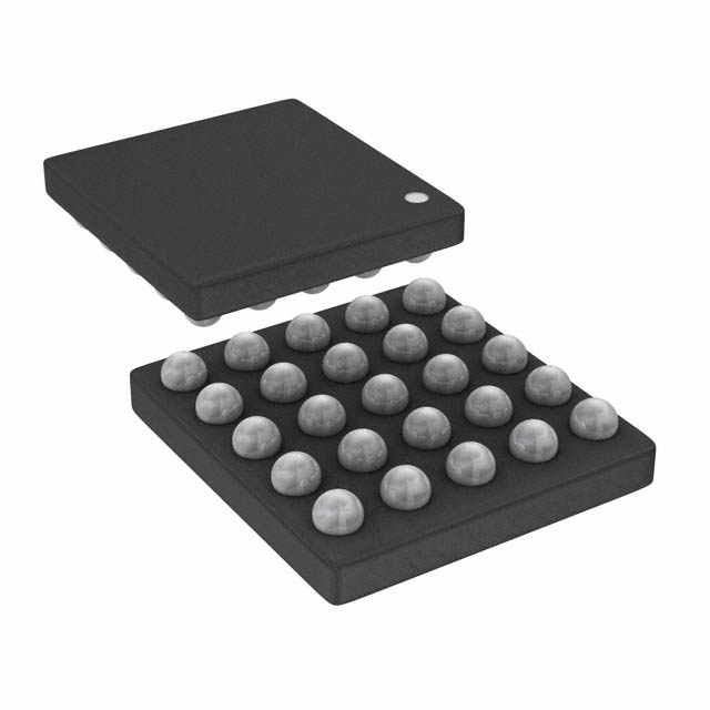
25-Lead, 2.1x2.1x0.625mm WLCSP Package
I2C™ is a trademark of NXP B.V. Corporation.
© 2008 Fairchild Semiconductor Corporation
FSA9480 • Rev. 1.0.6
www.fairchildsemi.com
FSA9480 — USB2.0 Accessory Switch
August 2010
�FSA9480 — USB2.0 Accessory Switch
Application Diagram
Figure 1. Typical Application
© 2008 Fairchild Semiconductor Corporation
FSA9480 • Rev. 1.0.6
www.fairchildsemi.com
2
�This block is used for factory-mode test and debug as described in Table 1.
Table 1.
Boot Table
Factory Mode
ID Resistor
JIG
UART, Boot Off
523KΩ
LOW
LOW
Table 3 - Accessory Auto Configuration Table
USB, Boot On
301KΩ
LOW
HIGH
Table 3 - Accessory Auto Configuration Table
USB, Boot Off
255KΩ
LOW
LOW
Table 3 - Accessory Auto Configuration Table
619KΩ
LOW
HIGH
Table 3 - Accessory Auto Configuration Table
N/A
Hi-Z
LOW
See Notes 1 and 2
UART, Boot On
No Factory Mode
BOOT
Switch Connections
Notes:
1. JIG pin description: Low signals the phone to power up. When disabled this open drain floats and the pin is Hi-Z
2. BOOT pin description: This boot pin level directs the baseband processor which mode to boot in when the JIG
box is attached, the JIG pin has been driven LOW, and the phone is powered up.
clamps the current, and reports to the baseband by
asserting OCP_EN in the Interrupt 1 Register. OCP
mode is only implemented when VBUS is provided by the
attached accessory. In PPD Mode (see below), the
FSA9480 does not limit current supplied by the phone.
D+, D- Charger Detection
This block monitors D+ and D- to determine when a
USB charger or dedicated charger is attached to the
phone. The detection scheme follows the dedicated
charger-detect algorithm as defined in the USB
Implementers Forum Battery Charging Working Group
specification titled Battery Charging Specification and
as described in the CEA-936-A USB car kit
specification. The FSA9480 distinguishes between a
dedicated charger and USB charger and reports the
appropriate type in the Device Type 1 Register.
Whenever either type of charger is detected, the
CHG_DET (ISET) pin is pulled LOW.
VBUS Detect and FET Blocks
This block monitors the status of the VBUS pin. A valid
VBUS level is defined as VBUS greater than 4.4V and less
than 5.5V. When VBUS is determined to be valid, the
internal NMOS charging FET is enabled, allowing
battery charging whenever a valid VBUS is present. The
charging FET is designed to limit inrush current to
100mA during enable to allow the voltage levels to
stabilize during initial connection. This current limiting is
automatic and designed per the requirements outlined
in the USB Battery Charging Specification.
Chip Power Select and Voltage Regulator
This block independently selects VBUS_IN or VBAT to
power the FSA9480 and includes necessary LDO
voltage regulators to provide stable power.
I2C™ and Digital Core Block
Valid ranges (for detecting and accepting supply) for:
VBAT: 3.0V to 4.4V
VBUS: 4.4V to 5.5V.
2
2
This block includes a full I C slave controller. The I C
2
slave fully complies with the I C specification version
2.1 requirements. This block also includes the FSA9480
chip master controller. The chip controller monitors
2
commands sent to the FSA9480 via I C from the
baseband and takes action. The FSA9480 digital core
takes inputs from the various functional blocks within
2
the FSA9480 and the I C commands received from the
phone baseband and relays relevant status updates to
the phone.
Voltage reference selection criteria:
If VBUS is present and in the valid range, the device
takes its power from VBUS. Otherwise, the device
takes its power from VBAT (if in valid range).
If the device is operating on VBAT and a valid VBUS
becomes available, the device switches to the VBUS
reference.
This block also accepts a VDDIO voltage reference for
baseband interface I/O signals.
ID Detector with Analog Digital Converter
(ADC) Block
This block monitors the ID pin for accessory attach and
detach. After determining which accessory has been
attached, the detector block reports this back to the
digital core, which sends an interrupt to the baseband.
Upon detecting changes in the ID pin voltage, the ADC
also writes the ADC value bits in the ADC Register. The
2
baseband processor can then read the I C registers
and
determine
the
appropriate
action.
The
programmable wait time does not begin until after the
baseband acknowledges the interrupt read. Figure 2
outlines the high-level accessory detection flow
sequence for Samsung-specific accessories.
OVP / OCP Shutdown Block
When VBUS is less than 6.8V, this block allows the VBUS
supply to enter the chip power select voltage regulator
block. For VBUS greater than 7.2V, the input is
disconnected, protecting the FSA9480 from excess
voltage. This block is capable of withstanding
continuous 28V in shutdown mode. Upon entering
shutdown, the OVP_EN bit in the Interrupt 1 Register is
set HIGH and an interrupt is sent to the baseband. The
Over-Current Protection (OCP) feature limits current
through the charger FET to ≤1.5A maximum. The
FSA9480 automatically senses an over-current event,
© 2008 Fairchild Semiconductor Corporation
FSA9480 • Rev. 1.0.6
FSA9480 — USB2.0 Accessory Switch
Block Descriptions
www.fairchildsemi.com
3
�FSA9480 — USB2.0 Accessory Switch
Accessory Detection Flow
Figure 2. Accessory Detection Flow Chart (Except USB)
Figure 3. USB Detection Flow Chart
Note:
3. Figure 2 applies to all accessories except USB; see Figure 3 for the USB accessory detection flow.
© 2008 Fairchild Semiconductor Corporation
FSA9480 • Rev. 1.0.6
www.fairchildsemi.com
4
�FSA9480 — USB2.0 Accessory Switch
Table 2.
ADC Selection Table
Bit Number
4
3
2
1
0
Equivalent RID
(KΩ)
0
0
0
0
0
GND
USB OTG Mode
0
0
0
0
1
2.000
Audio Send_End Button
0
0
0
1
0
2.604
Audio Remote S1 Button
0
0
0
1
1
3.208
Audio Remote S2 Button
0
0
1
0
0
4.014
Audio Remote S3 Button
0
0
1
0
1
4.820
Audio Remote S4 Button
0
0
1
1
0
6.030
Audio Remote S5 Button
0
0
1
1
1
8.030
Audio Remote S6 Button
0
1
0
0
0
10.030
Audio Remote S7 Button
0
1
0
0
1
12.030
Audio Remote S8 Button
0
1
0
1
0
14.460
Audio Remote S9 Button
0
1
0
1
1
17.260
Audio Remote S10 Button
0
1
1
0
0
20.500
Audio Remote S11 Button
0
1
1
0
1
24.070
Audio Remote S12 Button
0
1
1
1
0
28.700
Reserved Accessory #1
0
1
1
1
1
34.000
Reserved Accessory #2
1
0
0
0
0
40.200
Reserved Accessory #3
1
0
0
0
1
49.900
Reserved Accessory #4
1
0
0
1
0
64.900
Reserved Accessory #5
1
0
0
1
1
80.070
Audio Device Type 2
1
0
1
0
0
102.000
Phone Powered Device
1
0
1
0
1
121.000
TTY Converter
1
0
1
1
0
150.000
UART Cable
1
0
1
1
1
200.000
CEA-936-A Type-1 Charger
1
1
0
0
0
255.000
Factory Mode Boot OFF-USB
1
1
0
0
1
301.000
Factory Mode Boot ON-USB
1
1
0
1
0
365.000
Audio/Video Cable
1
1
0
1
1
442.000
CEA-936-A Type-2 Charger
1
1
1
0
0
523.000
Factory Mode Boot OFF-UART
1
1
1
0
1
619.000
Factory Mode Boot ON-UART
1
1
1
1
0
1
1
1
1
1
Description
(4)
(4)
(4)
1000.070
Audio Device Type 1 with Remote
1002.000
Audio Device Type 1 / Only Send-End
Open
(5)
USB Mode, Dedicated Charger or Accessory Detach
Notes:
4. Chargers must provide a valid VBUS for the FSA9480 to report them to the phone baseband.
5. Audio devices with remote and audio device / only send end are reported as audio in the Device Type 1
Register. The FSA9480 auto-configures in Audio Mode, as described in Table 3.
© 2008 Fairchild Semiconductor Corporation
FSA9480 • Rev. 1.0.6
www.fairchildsemi.com
5
�2
the switch auto configuration connections for the
various states is shown in Table 3.
The switch MUX block contains an I C controlled DP4T
multiplexer with dedicated paths for high-speed USB,
audio R/L, TV R/L, and UART signaling. A summary of
Table 3.
Accessory Auto Configuration Table
VBUS
DP
DM
ID
BOOT
JIG
CHG_DET
(ISET)
Audio Type 1
MIC
Audio_R
Audio_L
Key
Press
Monitor
LOW
Hi-Z
Hi-Z
Audio Type 2
Chg FET
Closed
RxD
TxD
(7)
LOW
Hi-Z
Hi-Z
(7)
Configuration Type
TTY
UART
MIC
Audio_R
LOW
Hi-Z
Hi-Z
(6)
RxD
TxD
(7)
LOW
Hi-Z
Hi-Z
USB
Chg FET
Closed
DP_Host
DM_Host
IDBP
LOW
Hi-Z
Hi-Z
USB Charger
Chg FET
Closed
DP_Host
DM_Host
IDBP
LOW
Hi-Z
Low
Video
LOW
Hi-Z
(6)
A/V Cable
Dedicated Charger, Car Kit
Type I & II Chargers
V_Audio_R V_Audio_L
Hi-Z
(8)
Chg FET
Closed
Open
Open
NA
LOW
Hi-Z
Low
Phone Powered Device
(PPD)
Chg FET
Closed
Audio_R
Audio_L
(7)
LOW
Hi-Z
Hi-Z
Boot_On
Chg FET
Open
RxD
TxD
(7)
HIGH
LOW
Hi-Z
Boot_Off
Chg FET
Open
RxD
TxD
(7)
LOW
LOW
Hi-Z
Boot_On
Chg FET
closed
DP_Host
DM_Host
(7)
HIGH
LOW
Hi-Z
Boot_Off
Chg FET
closed
DP_Host
DM_Host
(7)
LOW
LOW
Hi-Z
Factory Mode
Jig: UART
Factory Mode
Jig: USB
FSA9480 — USB2.0 Accessory Switch
Switch MUX Block
Notes:
6. If VBUS is valid, the charger FET is closed; otherwise, the charger FET is open.
7. ID is monitored by ADC for change of state.
8. Unless VBUS is valid, in which case, a charger adapter has been added and CHG_DET is enabled.
© 2008 Fairchild Semiconductor Corporation
FSA9480 • Rev. 1.0.6
www.fairchildsemi.com
6
�Initialization
CEA-936-A Car Kit
On initial power up, all register bits are initialized to their
2
default condition, as defined in the I C register map.
During initialization, all switch paths are open.
Immediately after initializing, all registers transition to
Standby/IDLE Mode.
Upon initial detection of a CEA-936-A car kit accessory,
the FSA9480 detects and reports a car kit accessory
attachment. The FSA9480 then initiates the car kit
signaling protocol, as described in the CEA-936-A
specification. Accordingly, the FSA9480 initializes in
UART mode, as described section 7.2.2 of the CEA936-A specification. The FSA9480 implements the fourwire protocol required for state transitions within the
CEA-936-A specification. The baseband processor
directs the FSA9480, using the mode bits in the Car Kit
Register, to signal the FSA9480 to change modes
within the car kit protocol. The phone generates the
USB, UART, and audio signals and the FSA9480
multiplexes the appropriate signal out to the attached
car kit device. The FSA9480 performs all handshaking
necessary with the attached car kit accessory and
automatically configures the switch MUX based on the
mode setting called for by the baseband processor. Car
Kit Audio Mode requires a 1.2V bias applied to the
audio signal. The FSA9480 contains a special audio
path that provides a 1.2V bias to the Audio_R and
Audio_L channels when in Car Kit Audio Mode. To
achieve the proper bias, the FSA9480 incorporates a
separate car kit audio path, containing two unity gain
amplifiers. The FSA9480 also uses these audio
amplifiers to implement the Car Kit Data During Audio
(DDA) Mode. While in DDA mode, the phone must limit
the audio signal being driven through the FSA9480 to
amplitude no greater than 1V, peak to peak.
VDDIO Reset Mode
While in active mode, the FSA9480 is reset by the
falling edge of the VDDIO signal pin as the VDDIO level
transitions from HIGH to LOW. In this case, the
FSA9480 automatically resets to its initialization state.
All register bits are initialized to their default condition,
2
as defined in the I C register map. Immediately
following VDDIO reset all switch paths are open and the
FSA9480 transitions to Standby/IDLE Mode. The
FSA9480 enters Standby/Idle Mode after the initial
reset, while the VDDIO pin remains LOW. Immediately
after the VDDIO level returns to a High and the Interrupt
Mask is cleared the FSA9480 reports any activity
detected while in Standby/Idle Mode.
I2C Reset Mode
The FSA9480 can also be reset by driving both the SDA
and SCL signal lines LOW for 30ms. In this case, the
FSA9480 automatically resets all registers to default
2
condition, as defined in the I C register map.
2
Immediately following I C reset, all switch paths are
open and FSA9480 transitions to Standby/IDLE mode.
2
See Figure 5 for detailed timing for I C Reset Mode.
Phone Powered Device Mode (PPD)
In Phone Power Device (PPD) Mode, the cell phone
provides power to the attached accessory through the
charger FET. In this mode, the charger FET is not
closed until after the wait time has expired; at which
time, the phone should have already biased its output
voltage level on the VBUS pin. The phone should never
source more than 10mA through the FSA9480 charger
FET while in PPD mode. When in PPD mode, the
charger FET provides a current path out of the phone to
the PPD. There is no inrush current limiting or OCP
protection provided by the charger FET when the
FSA9480 is in PPD Mode.
Standby / IDLE
In this state, no accessory is attached. This state is
connected to all other states. During this state, the
device is in a power-down mode with a minimal set of
functions running. The ID detector continuously
monitors the ID pin for accessory attach. Upon
accessory attach, the FSA9480 transitions to the
appropriate mode based on the accessory.
Charger Mode
When any of the possible charger types are attached,
the FSA9480 closes the FET switch and CHG_DET
(ISET) is asserted LOW. When CHG_DET is asserted
LOW this signals the phones charger IC to enable highcurrent mode. When CHG_DET is Hi-Z, the charger IC
defaults to low-current charge mode.
Audio Modes
When any of the compatible headsets are attached, the
FSA9480 configures as described in Table 3. The
FSA9480 is compatible with Samsung headphones that
include a remote-control feature. When in Audio Mode,
the FSA9480 continuously monitors for remote-control
button presses and reports any presses back to the
baseband. Figure 15 illustrates the headset with remote
basic circuit; Table 4 provides resistor values.
USB 2.0 and USB OTG Modes
When USB2.0 cable is attached, the FSA9480
configures the switch MUX block according to Table 3.
The charger FET is closed.
Audio Device Type-1 accessories are passive devices
with only one switch configuration per device. They may
or may not include a remote controller.
Dead Battery / No Battery Mode
When no battery or a dead battery is present, the
FSA9480 disables the following pins to Hi-Z: INTB,
2
2
I C_SDA, I C_SCL, Jig, Boot, RXD, TXD, and CHG_DET.
© 2008 Fairchild Semiconductor Corporation
FSA9480 • Rev. 1.0.6
FSA9480 — USB2.0 Accessory Switch
Mode Descriptions
www.fairchildsemi.com
7
�JIG Box Plug In
MUS Detects JIG
Box
MUS Auto
Configure
Switches Per
Table 4
MUS Writes
Device Register
and Asserts INTB
Factory Modes
MUS Enters
Standby
Factory Modes are initiated with the attachment of a
Samsung proprietary JIG Box and are used for phone
assembly and testing. The Factory Mode attach
procedure is slightly different from the standard
accessory attach flow. The primary difference is that the
© 2008 Fairchild Semiconductor Corporation
FSA9480 • Rev. 1.0.6
FSA9480 — USB2.0 Accessory Switch
FSA9480 automatically configures the switch paths as
soon as a Factory Mode accessory is attached and
VDDIO is present. This is unique in that the FSA9480
2
does not wait for an I C read acknowledge from the
baseband and does not employ the switch wait timer. A
second difference is that, in this mode, the JIG pin is
driven LOW even if the VDDIO pin is LOW. Figure 4
provides the attach flow for the JIG Box accessory.
Audio Device Type-2 devices include a built-in UART
controller and the FSA9480 auto configures with UART
switch paths connected, as described in Table 3. These
devices include a remote controller. After initial
configuration in UART Mode, the baseband may
change the FSA9480 switch mode configuration by
writing any of the following bit patterns in the Car Kit
Status Register mode bits: 000, 001, 100, 101. While
an audio type-2 accessory is attached, it is possible for
the baseband to signal changes in switch configuration
from any mode to any mode until device detach is
detected. While in DDA Mono (100) mode, the
FSA9480 DDA circuitry is activated, allowing data to be
sent and received during audio transmission between
the resident UART transceivers in the phone and the
audio type-2 device. The FSA9480 DDA audio scheme
follows that of the CEA-936-A specification as
implemented in the car kit mode of the FSA9480. Other
than implementing the DDA transmission and reception
scheme in CEA-936-A, the FSA9480 does not
implement any car kit protocols or state machines while
in Audio Device Type-2 Mode. In DDA Mode, the phone
must limit the audio signal driven through the FSA9480
to amplitude no greater than 1V, peak to peak.
Figure 4. JIG Box Detection Flow
www.fairchildsemi.com
8
�VBAT
VDDIO
SDA
30ms
SCL
30ms
Internal Reset Time
Idle Standby
Idle Standby
400µs
400µs
2
Figure 5. I C Reset Mode Timing
© 2008 Fairchild Semiconductor Corporation
FSA9480 • Rev. 1.0.6
FSA9480 — USB2.0 Accessory Switch
I2C Manual Reset Timing
www.fairchildsemi.com
9
�The FSA9480 follows the Interrupt guidelines as
described in the Samsung Interrupt Definition and
Default Path specification Rev 0.1 released July 15
2008. The baseband processor recognizes interrupt
signals by observing the falling edge of the INTB signal
in a high-to-low transition. During the phone power-up
2
sequence, VDDIO reset or I C reset the INTB pin is
masked on initialization and defaults LOW. After the
INTB mask is cleared by the baseband processor, the
INTB pin is HIGH in preparation of a future interrupt. If
2
the interrupt mask bit in the I C Control Register is
written HIGH when the system is already powered up,
the INTB remains HIGH until the INTB mask is cleared.
If an interruptible event occurs while the INTB pin is
masked, the FSA9480 changes the appropriate register
value and waits until the INTB mask bit is cleared, plus
the switch wait time before signaling an interrupt to the
baseband. Figure 6 illustrates the interrupt timing for the
FSA9480 during initial power up. Figure 7 shows the
INTB behavior during a VDDIO reset. Figure 8 illustrates
the INTB timing when the INT Mask bit is written by the
2
baseband using I C commands.
VBAT
VDDIO
9480_reset
FSA9480 — USB2.0 Accessory Switch
Interrupt Operation Description
INT mask clear
INT_Mask
INTB
INT event
INT read
Figure 6. Power-Up Interrupt Timing Diagram
VBAT
VDDIO
Standby
9480_reset
INT mask
INT_Mask
INTB
INT event
tSW
INT read
Switch Wait
RESET State = 100µs
Figure 7. VDDIO Reset Interrupt Timing Diagram
VBAT
VDDIO
INT mask
INT_Mask
INTB
INT Mask
written via
2
IC
command
INT
tsw
Switch Wait
Time
INT
read
2
Figure 8. INT Mask via I C Command Interrupt Timing Diagram
© 2008 Fairchild Semiconductor Corporation
FSA9480 • Rev. 1.0.6
www.fairchildsemi.com
10
�USB Cable Attach Timing
VBUS >4.0V
Charger FET Closed
USB Switches Closed
VBUS Voltage
XXXXXXXXXXXXXXXXXXXXXXXXXXXXXXXXXXXXXXXXXXXXXXXXX
FLOAT
FLOAT
ID Resistance
Charger FET RON
240ms
USB Path RON
400ms VBUS Debounce
120ms Charger
Detect
FSA9480 — USB2.0 Accessory Switch
Device Attach Timing Diagrams
Figure 9. USB Cable Attach Timing Diagram
Figure 10.
ID Based Accessories Attach Timing
JIG Box Attach Timing (VBUS Present)
VBUS >4.0V
Vbus Voltage
ID Resistance
FLOAT
XXXXXXXX
JIG Pin
VBUS valid debounce 400ms
ID detection time 600ms
BB wake-up
time
VDDIO
BOOT Pin
Figure 11.
© 2008 Fairchild Semiconductor Corporation
FSA9480 • Rev. 1.0.6
JIG Box Attach Timing (VBUS Present)
www.fairchildsemi.com
11
�Figure 12.
Figure 13.
JIG Box Attach Timing (No VBUS)
FSA9480 — USB2.0 Accessory Switch
Device Attach Timing Diagrams (Continued)
Dedicated Charger (TA) Attach Timing
USB Charging Host Port Attach Timing
Charger FET Closed
INTB Asserted and
registers written
VBUS >4.0V
VBUS Voltage
XXXXXXXXXXXXXXXXXXXXXXXXXXXXXXXXXXXXXXXXXXXXXXXXX
FLOAT
FLOAT
ID Resistance
VBUS_OUT
240ms
Switch RON
CHG_DET Pin
100ms
INTB Pin
VBUS valid debounce 400ms
Figure 14.
© 2008 Fairchild Semiconductor Corporation
FSA9480 • Rev. 1.0.6
CHG DETECTION 160ms
USB Charging Host Port Attach Timing
www.fairchildsemi.com
12
�FSA9480 — USB2.0 Accessory Switch
Audio Type 1 and 2 Remote Control Configuration
Figure 15.
Table 4.
Stereo Headset with Remote Configuration
Remote Control Resistor Table (1% Resistor Values)
Switch and Resistor Number
Resistor Value
Resistor Number
Resistor Value
RSE
2KΩ
B7, R7
2KΩ
B1, R1
0.604KΩ
B8, R8
2KΩ
B2, R2
0.604KΩ
B9, R9
2.43KΩ
B3, R3
0.806KΩ
B10, R10
2.8KΩ
B4, R4
0.806KΩ
B11, R11
3.24KΩ
B5, R5
1.21KΩ
B12, R12
3.57KΩ
B6, R6
2KΩ
RID
© 2008 Fairchild Semiconductor Corporation
FSA9480 • Rev. 1.0.6
976KΩ (Audio Type 1)
56KΩ (Audio Type 2)
www.fairchildsemi.com
13
�FSA9480 — USB2.0 Accessory Switch
Key Press Timing Diagrams
Figure 16.
Figure 17.
© 2008 Fairchild Semiconductor Corporation
FSA9480 • Rev. 1.0.6
Regular Key Press Timing Diagram
Long Key Press Timing Diagram
www.fairchildsemi.com
14
�FSA9480 — USB2.0 Accessory Switch
Marking Information
Z
= Assembly Plant Code
X
= Year
Y
= Work Week
KK = Lot Trace Code
N4 = Product Identifier
Figure 18.
Top Mark with Pin A1 Orientation
Pin Configuration
Figure 19.
25-Pin, WLCSP Pin Assignments (Top Through View)
Pin Map
Column 1
Row A
Row B
INTB
DP_Host
Column 2
Column 3
Column 4
Column 5
VDDIO
CHG_DET
VBUS_OUT
VBUS_IN
2
Audio_L
MIC
DM_CON
2
I C_SDA
Row C
DM_Host
I C_SCL
V_Audio_L
Audio_R
DP_CON
Row D
VBAT
ID_Bypass
V_Audio_R
Video
ID_CON
Row E
RxD
TxD
BOOT
JIG
GND
© 2008 Fairchild Semiconductor Corporation
FSA9480 • Rev. 1.0.6
www.fairchildsemi.com
15
�Name
Pin # Type
Default
State
Description
USB Interface
DP_Host
B1
Signal
Path
Open
D+ signal, dedicated USB port to be connected to the resident USB
transceiver on the phone
DM_Host
C1
Signal
Path
Open
D- signal, dedicated USB port to be connected to the resident USB
transceiver on the phone
ID_Bypass
D2
Signal
Path
Open
USB ID pin bypass allows the FSA9480 to pass the ID signal pin through
to the resident phone USB controller when a USB accessory is attached
Audio Interface
Audio_L
B3
Signal
Path
Open
Left audio channel from phone audio-out codec
Audio_R
C4
Signal
Path
Open
Right audio channel from phone audio-out codec
MIC
B4
Signal
Path
Open
Connected to the phone audio codec MIC input pin
FSA9480 — USB2.0 Accessory Switch
Pin Descriptions
Video Interface
Video
D4
Signal
Path
Open
Input signal driven by the phone DMB video-out signal
V_Audio_L
C3
Signal
Path
Open
Left audio channel from TV audio out
V_Audio_R
D3
Signal
Path
Open
Right audio channel from TV audio out
UART Interface
TxD
E2
Signal
Path
Open
Tx connection from resident UART transceiver on the phone
RxD
E1
Signal
Path
Open
Rx connection from resident UART transceiver on the phone
Factory Interface
Jig
E4
OpenDrain
Output
Hi-Z
Output control signal driven by the FSA9480; used by the processor for
Samsung factory test modes
Boot
E3
PushPull
Output
LOW
Output control signal driven by the FSA9480, used by the processor for
Samsung factory test modes
Power Interface
VBAT
D1
Power
N/A
Input voltage supply pin to be connected to the phone battery output
VBUS_OUT
A4
Power
N/A
Output voltage supply pin to be connected to the source voltage pin on
the charger IC
VDDIO
A2
Power
N/A
Input baseband interface I/O supply pin
CHG_DET
(ISET)
A3
OpenDrain
Output
Hi-Z
Open-drain I/O pin, active LOW, used to signal charger IC that a charger
has been attached
Continued on the following page…
© 2008 Fairchild Semiconductor Corporation
FSA9480 • Rev. 1.0.6
www.fairchildsemi.com
16
�Name
Pin # Type
Default
State
Description
Connector Interface
VBUS_IN
A5
Power
N/A
Input voltage supply pin; connect to the VBUS pin of the USB connector
GND
E5
Power
N/A
Ground
ID_CON
D5
Signal
Path
Open
Connected to the USB connector ID pin; depending on the FSA9480
state, this pin can share ID or video signals
DP_CON
C5
Signal
Path
Open
Connected to the USB connector D+ pin; depending on the FSA9480
signaling mode, this pin can share D+, S_R, V_R, Rxd, or MIC signals
DM_CON
B5
Signal
Path
Open
Connected to the USB connector D- pin; depending on the FSA9480
signaling mode, this pin can share D-, S_L, Txd, or V_L signals
2
C2
Input
N/A
I C serial clock signal to be connected to the phone based I C master
I C_SDA
2
B2
OpenDrain
I/O
Hi-Z
Open-drain I/O pin; I C serial data signal to be connected to the phone
2
based I C master
INTB
A1
PushPull
Output
Low
Interrupt signal to prompt the phone baseband to read the I C register
bits, indicates a change in ID pin status or accessory attach status
2
I C Interface
I C_SCL
© 2008 Fairchild Semiconductor Corporation
FSA9480 • Rev. 1.0.6
2
2
FSA9480 — USB2.0 Accessory Switch
Pin Descriptions (Continued)
2
2
www.fairchildsemi.com
17
�Stresses exceeding the absolute maximum ratings may damage the device. The device may not function or be
operable above the recommended operating conditions and stressing the parts to these levels is not recommended.
In addition, extended exposure to stresses above the recommended operating conditions may affect device
reliability. The absolute maximum ratings are stress ratings only.
Symbol
Parameter
Min.
VBAT/VDDIO Supply Voltage from Battery / Baseband
VBUS
IIK
Switch I/O Voltage
-0.5
6.0
V
28.0
V
-1.0
VBUS+0.5
Stereo/Mono Audio Path Active
-1.5
VBAT+0.5
All Other Channels
-0.5
VBAT+0.5
Input Clamp Diode Current
-50
Chg_Det Charger Detect Sets Current Sink Capability of the Charger IC
ISW
ISWPEAK
Switch I/O Current (Continuous)
V
mA
30
USB
50
Audio
60
mA
mA
All Other Channels
50
USB
150
mA
150
mA
1.2
A
Peak Switch Current (Pulsed at 1ms Audio
Duration, 2V
0
VDDIO