Is Now Part of
To learn more about ON Semiconductor, please visit our website at
www.onsemi.com
Please note: As part of the Fairchild Semiconductor integration, some of the Fairchild orderable part numbers
will need to change in order to meet ON Semiconductor’s system requirements. Since the ON Semiconductor
product management systems do not have the ability to manage part nomenclature that utilizes an underscore
(_), the underscore (_) in the Fairchild part numbers will be changed to a dash (-). This document may contain
device numbers with an underscore (_). Please check the ON Semiconductor website to verify the updated
device numbers. The most current and up-to-date ordering information can be found at www.onsemi.com. Please
email any questions regarding the system integration to Fairchild_questions@onsemi.com.
ON Semiconductor and the ON Semiconductor logo are trademarks of Semiconductor Components Industries, LLC dba ON Semiconductor or its subsidiaries in the United States and/or other countries. ON Semiconductor owns the rights to a number
of patents, trademarks, copyrights, trade secrets, and other intellectual property. A listing of ON Semiconductor’s product/patent coverage may be accessed at www.onsemi.com/site/pdf/Patent-Marking.pdf. ON Semiconductor reserves the right
to make changes without further notice to any products herein. ON Semiconductor makes no warranty, representation or guarantee regarding the suitability of its products for any particular purpose, nor does ON Semiconductor assume any liability
arising out of the application or use of any product or circuit, and specifically disclaims any and all liability, including without limitation special, consequential or incidental damages. Buyer is responsible for its products and applications using ON
Semiconductor products, including compliance with all laws, regulations and safety requirements or standards, regardless of any support or applications information provided by ON Semiconductor. “Typical” parameters which may be provided in ON
Semiconductor data sheets and/or specifications can and do vary in different applications and actual performance may vary over time. All operating parameters, including “Typicals” must be validated for each customer application by customer’s
technical experts. ON Semiconductor does not convey any license under its patent rights nor the rights of others. ON Semiconductor products are not designed, intended, or authorized for use as a critical component in life support systems or any FDA
Class 3 medical devices or medical devices with a same or similar classification in a foreign jurisdiction or any devices intended for implantation in the human body. Should Buyer purchase or use ON Semiconductor products for any such unintended
or unauthorized application, Buyer shall indemnify and hold ON Semiconductor and its officers, employees, subsidiaries, affiliates, and distributors harmless against all claims, costs, damages, and expenses, and reasonable attorney fees arising out
of, directly or indirectly, any claim of personal injury or death associated with such unintended or unauthorized use, even if such claim alleges that ON Semiconductor was negligent regarding the design or manufacture of the part. ON Semiconductor
is an Equal Opportunity/Affirmative Action Employer. This literature is subject to all applicable copyright laws and is not for resale in any manner.
�特性
应用
• 通过 UL 第 E209204 号认证 (UL1557)
• 小功率交流电机驱动器的三相逆变器驱动
• 高性能 PQFN 封装
相关资料
• 500 V RDS(on) = 2.2 (最大值) FRFET MOSFET 三
相逆变器,带有栅极驱动器和保护功能
• AN-9077 - Motion SPM® 7 Series User’s Guide
• AN-9078 - Surface Mount Guidelines for Motion
SPM® 7 Series
• 低端 MOSFET 的三个独立开源引脚用于三相电流感测
• 高电平有效接口,可用于 3.3 / 5 V 逻辑电平,施密特触
发脉冲输入
概述
FSB70450 是一款先进的 Motion SPM® 7 模块,为交流
感应、无刷直流电机和 PMSM 电机提供非常全面的高性
能逆变器输出平台。这些模块综合优化了内置 MOSFETs
(FRFET® 技术)的栅极驱动以最小化电磁干扰和能量损
耗。同时也提供多重模组保护特性,集成欠压闭锁,热量
监测,故障报告和互锁功能。内置的一个 HVIC 将逻辑电
平栅极输入转化为适合驱动模块内部 MOSFET 的高电
压,高电流驱动信号。独立的开源 MOSFET 端子在每个
相位均有效,可支持大量不同种类的控制算法。
• 针对低电磁干扰进行优化
• 内置于 HVIC 的温度感测
• 用于栅极驱动,互锁功能和欠压保护的 HVIC
• 绝缘等级:1500 Vrms / 分钟
• 湿度敏感等级 (MSL) 3
• 符合 RoHS 标准
封装标识与定购信息
器件标识
器件
封装
卷尺寸
卷带宽度
数量
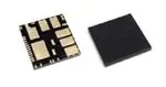
FSB70450
FSB70450
PQFN27A
13’’
24 mm
1000 个
©2013 飞兆半导体公司
FSB70450 Rev. 1.1
1
www.fairchildsemi.com
FSB70450 Motion SPM® 7 系列
2015 年12 月
FSB70450
Motion SPM® 7 系列
�逆变器部分 (单个 MOSFET,除非另有说明。)
符号
参数
工作条件
额定值
单位
500
V
VDSS
单个 MOSFET 的漏极 — 源极电压
*ID 25
单个 MOSFET 的漏极持续电流
TCB = 25°C (注 1)
4.8
A
*ID 80
单个 MOSFET 的漏极持续电流
TCB = 80°C
3.6
A
*IDP
单个 MOSFET 的漏极峰值电流
TCB = 25°C, PW < 100 s
9.7
A
*PD
最大功耗
TCB = 25°C,单个 MOSFET
110
W
额定值
单位
控制部分 (单个 HVIC,除非另有说明。)
符号
参数
工作条件
VDD
控制电源电压
施加在 VDD 和 COM 之间
20
V
VBS
高端偏压
施加在 VB 和 VS 之间
20
V
VIN
输入信号电压
施加在 IN 和 COM 之间
-0.3 ~ VDD + 0.3
V
VFO
故障输出电源电压
施加在 FO 和 COM 之间
-0.3 ~ VDD + 0.3
V
IFO
故障输出电流
灌电流 FO 引脚
电流感测输入电压
施加在 Csc 和 COM 之间
VCSC
5
mA
-0.3 ~ VDD + 0.3
V
额定值
单位
整个系统
符号
参数
工作条件
TJ
工作结温
-40 ~ 150
°C
TSTG
存储温度
-40 ~ 125
°C
VISO
绝缘电压
1500
Vrms
60 Hz,正弦波形, 1 分钟,连接陶
瓷基板到引脚
注:
1. TCB 是壳体底部的垫片温度。
2. 标记为 “ * “ 的为计算值或设计因素。
©2013 飞兆半导体公司
FSB70450 Rev. 1.1
2
www.fairchildsemi.com
FSB70450 Motion SPM® 7 系列
绝对最大额定值
�FSB70450 Motion SPM® 7 系列
引脚描述
引脚号
引脚名
1
/FO
故障输出
引脚描述
2
VTS
以电压形式输出的 HVIC 温度
3
Cfod
用于故障输出持续时间的电容
4
Csc
短路电流感测输入电容 (低通滤波器)
5
VDD
驱动 IC 和 MOSFET 的电源偏置电压
6
IN_UH
高端 U 相的信号输入
7
IN_VH
高端 V 相的信号输入
8 (8a)
COM
9
IN_WH
高端 W 相的信号输入
10
IN_UL
低端 U 相的信号输入
11
IN_VL
低端 V 相的信号输入
12
IN_WL
低端 W 相的信号输入
13
Nu
U 相的直流输入负端
14
U
U 相输出
15
Nv
V 相的直流输入负端
公共电源接地
16
V
V 相输出
17
W
W 相输出
18
Nw
19
VS(W)
20
PW
W 相的直流输入正端
21
PV
V 相的直流输入正端
22
PU
U 相的直流输入正端
23 (23a)
VS(V)
V 相 MOSFET 驱动的高端偏压接地
24 (24a)
VS(U)
U 相 MOSFET 驱动的高端偏压接地
25
VB(U)
U 相 MOSFET 驱动的高端偏压
26
VB(V)
V 相 MOSFET 驱动的高端偏压
27
VB(W)
W 相 MOSFET 驱动的高端偏压
W 相的直流输入负端
W 相 MOSFET 驱动的高端偏压接地
(19) V S(W)
(23), (23a) V S(V)
(24), (24a) V S(U)
OUT(UH)
(25) V B(U)
(26) V B(V)
(27) V B(W)
(22) Pu
(21) Pv
(20) Pw
VB(U)
VS(U)
VB(V)
(14) U
VB(W)
OUT(VH)
VS(V)
(5) V DD
(8),(8a) COM
(6) IN_UH
(7) IN_VH
(9) IN_WH
(10) IN_UL
(11) IN_VL
(12) IN_WL
(1) /Fo
(2) V TS
(3) Cfod
(4) Csc
(16) V
V DD
COM
OUT(WH)
UH
VS(W)
VH
(17) W
WH
UL
OUT(UL)
VL
(13) Nu
WL
/Fo
OUT(VL)
V TS
Cfod
(15) Nv
Csc
OUT(WL)
(18) Nw
图 1. 引脚布局和内部框图
注:
4. 每个低端 MOSFET 的源极端子与 Motion SPM® 7 中的电源接地或偏压接地不连接。外部连接应当如图 2 所示。
5. 后缀为 -a 的垫片连接到相同数字的引脚,例如:8 和 8a 在内部连接在一起。
©2013 飞兆半导体公司
FSB70450 Rev. 1.1
3
www.fairchildsemi.com
�逆变器部分 (单个 MOSFET,除非另有说明。)
符号
参数
工作条件
最小值 典型值 最大值
500
BVDSS
漏极-源极击穿电压
VIN = 0 V, ID = 1 mA (注 1)
IDSS
零栅极电压漏极电流
VIN = 0 V, VDS = 500 V
-
漏极至源极静态导通电阻
VDD = VBS = 15 V, VIN = 5 V, ID = 1.0 A
-
漏极-源极二极管正向电压
VDD = VBS = 15V, VIN = 0 V, ID = -1.0 A
RDS(on)
VSD
-
单位
-
V
-
1
mA
1.9
2.2
-
0.9
1.2
V
tON
-
600
-
ns
tD(ON)
-
560
-
ns
tOFF
-
660
-
ns
-
600
-
ns
-
1.9
-
A
tD(OFF)
Irr
VPN = 300 V, VDD = VBS = 15 V, ID = 1.0 A
VIN = 0 V 5 V,电感负载 L = 3 mH
低端 MOSFET 开关
(注 2)
开关时间
trr
-
90
-
ns
EON
-
45
-
J
EOFF
-
8
-
J
控制部分 (单个 HVIC,除非另有说明。)
符号
IQDD
参数
VDD 静态电流
工作条件
最小值 典型值 最大值
单位
VDD=15 V, VIN=0 V
VDD - COM
-
1.7
3.0
mA
-
45
70
A
IQBS
VBS 静态电流
VBS=15 V, VIN=0 V
VB(X)-VS(X), VB(V)VS(V), VB(W)-VS(W)
IPDD
VDD 工作电流
VDD=15 V, FPWM=20
kHz,duty=50%,PWM
信号低端输入
VDD - COM
-
1.9
3.2
mA
IPBS
VBS 工作电流
VBS=15 V, FPWM=20
kHz,duty=50%,PWM
信号高端输入
VB(U)-VS(U), VB(V)VS(V), VB(W)-VS(W)
-
300
400
A
VDD 欠压保护检测电平
7.4
8.0
9.4
V
VDD 欠压保护复位电平
8.0
8.9
9.8
V
VBS 欠压保护检测电平
7.4
8.0
9.4
V
VBS 欠压保护复位电平
8.0
8.9
9.8
V
UVDDD
UVDDR
UVBSD
低端欠压保护 (图 6)
高端欠压保护 (图 7)
UVBSR
VTS
HVIC 温度感测电压输出
VDD=15 V, THVIC=25°C (注 3)
VIH
导通阈值电压
逻辑高电平
VIL
关断阈值电压
逻辑低电平
短路电流保护触发电平
VDD=15 V
故障输出脉宽
CFOD=33 nF (注 4)
VSC(ref)
tFOD
IN - COM
CSC - COM
580
675
770
mV
-
-
2.4
V
0.8
-
-
V
0.45
0.5
0.55
V
1.0
1.4
1.8
ms
注:
1. BVDSS 是 Motion SPM® 7 产品中的单个 MOSFET 的漏极和源极端子之间的绝对最大额定电压。考虑到寄生电感,VPN 应远低于该值,因此 VPN 在任何情况下不得超过 BVDSS。
2. tON 和 tOFF 包括内部驱动 IC 的传输延迟。所列出的数值是在实验室测试条件下测得,在实际应用中因为印刷电路板和布线的差异,数值也会有所不同。请参阅图 3 介绍的开关
时间定义,以及图 4 中的开关测试电路。
3. Vts 只能用作模块的温度感测,但不能自动关闭 MOSFETs。
4. 故障输出脉宽 tFOD 取决于电容 CFOD 的值,可采用下面的近似公式进行计算:CFOD = 24 x 10-6 x tFOD [F]
©2013 飞兆半导体公司
FSB70450 Rev. 1.1
4
www.fairchildsemi.com
FSB70450 Motion SPM® 7 系列
电气特性 (TJ = 25°C, VDD = VBS = 15 V 除非另有说明。)
�符号
参数
工作条件
最小值 典型值 最大值
单位
VPN
电源电压
施加在 P 和 N 之间
-
300
400
V
VDD
控制电源电压
施加在 VDD 和 COM 之间
13.5
15.0
16.5
V
VBS
高端偏压
施加在 VB 和 VS 之间
13.5
15.0
16.5
V
-1.0
-
1.0
V/s
500
-
-
ns
-
15
-
kHz
dVDD/dt,
dVBS/dt
控制电源波动
tdead
防止桥臂直通的死区时间
VDD = VBS = 13.5 ~ 16.5 V, TJ 150°C
fPWM
PWM 开关频率
TJ 150°C
热阻
符号
RJCB
参数
工作条件
最小值 典型值 最大值
单个 MOSFET 工作条件下
(注 1)
结点 — 壳体底部的热阻
5-V
Line
-
These values depend on PWM
control algorithm
15-V
Line
0.9
-
单位
°C/W
One-Leg Diagram of SPM
C1
V DD
R5
Micom
P
VB
HIN
HO
LIN
VS
V PN
Inverter
Output C3
/Fo
C5
V TS
LO
C SC
C4
N
R3
COM
10F
C2
C6
R2
* Example of bootstrap paramters:
C 1 = C 2 = 1 F ceramic capacitor,
图 2. 推荐的 MCU 接口和自举电路及其参数
注:
1. RJCB 是根据应用电路板布局得出的模拟值。(请参考用户指导手册 SPM7 系列)
2. 自举电路的参数取决于 PWM 算法。上述为开关频率为 15 kHz 时的参数的典型例子。
3. (虚线显示部分)每个输入端的 RC 耦合 (R5 和 C5),可用于防止由浪涌噪声产生的错误输入信号。 SPM® 的信号输入与标准 COMS 或 LSTTL 的输出兼容。
4. 印刷电路板图形中的粗线应尽量短且粗,以减少电路中的寄生电感,从而导致浪涌电压的降低。
©2013 飞兆半导体公司
FSB70450 Rev. 1.1
5
www.fairchildsemi.com
FSB70450 Motion SPM® 7 系列
推荐工作条件
�ID
120%
FSB70450 Motion SPM® 7 系列
100%
ID
t rr
Irr
V
V
ID
D S
ID
V
IN
V
D S
IN
0
tD
tO
V
IN (O N )
tD
(O N )
(O F F )
tO
N
10%
ID
90%
V
ID
F F
90%
IN (O F F )
ID
10%
ID
(b ) T u rn -o ff
(a ) T u rn -o n
图 3. 开关时间的定义
5-V
Line
15-V
Line
ID
VDD
VB
HIN
HO
LIN
VS
/Fo
LO
L
VDC
+
V DS
-
VTS
COM
图 4. 开关测试电路 (低端)
Input Signal
UV Protection
Status
High-side/Low-side
RESET
DETECTION
RESET
UV BSR(DDR)
UV BSD(DDD)
MOSFET Drain Current
Fault Output
(Only Low-side UV protection)
图 5. 欠压保护
©2013 飞兆半导体公司
FSB70450 Rev. 1.1
6
www.fairchildsemi.com
�c6
Protection
Circuit state
SET
Internal MOSFET
Gate-Source Voltage
c3
FSB70450 Motion SPM® 7 系列
Control input
c7
RESET
c4
c2
SC
c1
c8
Output Current
SC Reference Voltage
Sensing Voltage
of the shunt
resistance
CR circuit time
constant delay
Fault Output Signal
c5
图 6. 短路电流保护
(包含外部分流电阻和 CR 连接)
c1:正常工作:MOSFET 导通并加载电流。
c2:短路电流检测 (SC 触发)。
c3:MOSFET 栅极硬中断。
c4:MOSFET 关断。
c5:故障输出延时工作启动:故障持续时间 (tFOD)。
c6:输入 “L”:MOSFET 关断状态。
c7:输入 “H”:MOSFET 导通状态,但是在故障输出有效的时间内, MOSFET 不导通。
c8:MOSFET 关断状态。
Hin
Lin
Ho
Lo
图 7. 互锁功能的时间图
©2013 飞兆半导体公司
FSB70450 Rev. 1.1
7
www.fairchildsemi.com
�FSB70450 Motion SPM® 7 系列
Tem p erature S ensing V o ltag e, V T S [V ]
4.0
Min.
Typ.
Max.
3.5
Typ. 2.57V@ 125 °
C
3.0
2.5
Typ . 2.10V@ 100 °
C
2.0
125±5 °
C
100±5 °
C
1.5
Typ. 1.15V @ 50 °
C
1.0
50±5 °
C
0.5
0.0
0
25
50
75
100
125
150
175
H VIC Tem perature, T H V IC [°C]
图 8. 温度曲线 VTS vs. THVIC
VS(W)
VS(V)
VS(U)
C1
VB(U)
VB(V)
VB(W)
P
OUT(UH)
VB(U)
VS(U)
VB(V)
U
VB(W)
OUT(VH)
VS(V)
15V
5V
C2
R5
VDD
VDD
COM
COM
/Fo
IN_UH
IN_VH
IN_WH
IN_UL
IN_VL
IN_WL
MCU
C5
C8
C4
VTS
Cfod
Csc
C7
V
M
C3 VDC
OUT(WH)
VS(W)
W
OUT(UL)
/Fo
Nu
UH
VH
WH
OUT(VL)
UL
Nv
VL
R3
WL
Vts
OUT(WL)
Nw
Cfod
Csc
R2
C6
图 9. 应用电路实例
注:
1. Motion SPM® 7 产品和 MCU 的每个输入端的 RC 耦合 (R5 和 C5, R2 和 C6)和 C1, C5, C7, C8,能有效的防止由浪涌噪声产生的错误的输入信号。
2. 为避免浪涌电压和 HVIC 故障,接地线和输出端子之间的接线应短且粗。
3. 所有的滤波电容器应紧密连接到 Motion SPM 7 产品,它们应当具有能够很好的阻挡高频纹波电流的特性。
©2013 飞兆半导体公司
FSB70450 Rev. 1.1
8
www.fairchildsemi.com
�8 9 10 11 12
13
0.65
3 4 5
1 2
6.45
5.85
5.60
5.05
4.50
4.75
5.28
5.55
5.80
6.08
0.75(9X)
0.55
C A B
1.35
0.00
0.25
4.70
4.60
5.80
6.45
0.10
6
7
27
5.80
4.75
14
26
3.90
0.40(26X)
0.20
8a
(1.15)
1.85
1.55
1.15
15
2.85
2.25
2.05
16
1.00
0.60
25
(1.50)
24
0.45
0.00
0.15
0.20
0.30
(1.60)
24a
23
23a
16
0.65
0.80
1.20
1.10
2.50
2.75
2.90
22
4.40
22
2.25
2.65
17
17
5.95
4.05
4.45
4.90
5.60
6.10
6.45
22
20
20
0.35
0.15
(4X)
19
18
18
0.35 (6X)
0.15
4.53
2.75
3.25
1.65
1.45
1.70
21
1.20
1.00
0.40
3.80
3.20
5.07
6.45
6.10
2.50
21
22
BOTTOM VIEW
21
22
13.00
12.80
PKG
CL
21
20
SCALE: 2:1
A
20
19
18
B
18
22
22
22
PKG CL23
0.10 C
17
17
16
23a
24a
16
24
25
13.00
12.80
1.40
1.20
0.08 C
C
0.30
0.20
0.05
0.00
15
8a
14
26
27
PIN 1
QUADRANT
0.10 C
1.40
1.20
1 2 3 4 5 6 7 8 9 10 11 12
TOP VIEW
SEE DETAIL 'A'
FRONT VIEW
13
SCALE: 2:1
SEATING
PLANE
�6.10
6.13
6.88
4.50
1.55
1.73
3.00
0.00
2.50
2.03
1.05
0.97
0.42
3.77
3.22
5.07
6.12
6.88
0.35
22
21
21
0.55
20
20
19
18
18
6.88
22
6.13
0.35
TYP
22
4.40
17
22
2.73
2.48
1.55
0.98
0.20
0.00
0.48
23
0.70
0.65
2.65
2.23
16
1.23
0.80
16
24
1.15
1.53
1.85
17
1.65
23a
24a
1.05
25
15
1.11 (9X)
8a
26
4.50
5.08
14
27
5.85
0.35
1 2 3
0.65
TYP
4
5 6
7 8
9 10 11 12
13
6.13
5.58
4.88
4.48
4.05
0.60
1.03
2.03
2.23
2.88
3.42
3.88
4.78
5.58
5.78
6.23
6.88
LAND PATTERN
RECOMMENDATION
SCALE: 2:1
NOTES: UNLESS OTHERWISE SPECIFIED
A) THIS PACKAGE IS NOT PRESENTLY
REGISTERED TO ANY STANDARD
COMMITTEE.
B) DIMENSIONS DO NOT INCLUDE BURRS OR
MOLD FLASH. MOLD FLASH OR BURRS DOES
NOT EXCEED 0.10MM.
C) ALL DIMENSIONS ARE IN MILLIMETERS.
D) DRAWING CONFORMS TO ASME Y14.5M-1994.
E) LAND PATTERN REFERENCE:
QFN65P1290X1290X140-40N-40N
F) DRAWING FILE NAME: MKT-PQFN27AREV3.
G) IT IS NOT NECESSARY TO SOLDER 23a AND
24a, AND CAN BE OMITTED FROM THE
FOOTPRINT
H) FAIRCHILD SEMICONDUCTOR
4.78
5.25
5.80
6.10
2.70
2.73
1.33
0.10
0.28
4.72
4.63
5.78
0.30
�ON Semiconductor and
are trademarks of Semiconductor Components Industries, LLC dba ON Semiconductor or its subsidiaries in the United States and/or other countries.
ON Semiconductor owns the rights to a number of patents, trademarks, copyrights, trade secrets, and other intellectual property. A listing of ON Semiconductor’s product/patent
coverage may be accessed at www.onsemi.com/site/pdf/Patent−Marking.pdf. ON Semiconductor reserves the right to make changes without further notice to any products herein.
ON Semiconductor makes no warranty, representation or guarantee regarding the suitability of its products for any particular purpose, nor does ON Semiconductor assume any liability
arising out of the application or use of any product or circuit, and specifically disclaims any and all liability, including without limitation special, consequential or incidental damages.
Buyer is responsible for its products and applications using ON Semiconductor products, including compliance with all laws, regulations and safety requirements or standards,
regardless of any support or applications information provided by ON Semiconductor. “Typical” parameters which may be provided in ON Semiconductor data sheets and/or
specifications can and do vary in different applications and actual performance may vary over time. All operating parameters, including “Typicals” must be validated for each customer
application by customer’s technical experts. ON Semiconductor does not convey any license under its patent rights nor the rights of others. ON Semiconductor products are not
designed, intended, or authorized for use as a critical component in life support systems or any FDA Class 3 medical devices or medical devices with a same or similar classification
in a foreign jurisdiction or any devices intended for implantation in the human body. Should Buyer purchase or use ON Semiconductor products for any such unintended or unauthorized
application, Buyer shall indemnify and hold ON Semiconductor and its officers, employees, subsidiaries, affiliates, and distributors harmless against all claims, costs, damages, and
expenses, and reasonable attorney fees arising out of, directly or indirectly, any claim of personal injury or death associated with such unintended or unauthorized use, even if such
claim alleges that ON Semiconductor was negligent regarding the design or manufacture of the part. ON Semiconductor is an Equal Opportunity/Affirmative Action Employer. This
literature is subject to all applicable copyright laws and is not for resale in any manner.
PUBLICATION ORDERING INFORMATION
LITERATURE FULFILLMENT:
Literature Distribution Center for ON Semiconductor
19521 E. 32nd Pkwy, Aurora, Colorado 80011 USA
Phone: 303−675−2175 or 800−344−3860 Toll Free USA/Canada
Fax: 303−675−2176 or 800−344−3867 Toll Free USA/Canada
Email: orderlit@onsemi.com
© Semiconductor Components Industries, LLC
N. American Technical Support: 800−282−9855 Toll Free
USA/Canada
Europe, Middle East and Africa Technical Support:
Phone: 421 33 790 2910
Japan Customer Focus Center
Phone: 81−3−5817−1050
www.onsemi.com
1
ON Semiconductor Website: www.onsemi.com
Order Literature: http://www.onsemi.com/orderlit
For additional information, please contact your local
Sales Representative
www.onsemi.com
�