Is Now Part of
To learn more about ON Semiconductor, please visit our website at
www.onsemi.com
Please note: As part of the Fairchild Semiconductor integration, some of the Fairchild orderable part numbers
will need to change in order to meet ON Semiconductor’s system requirements. Since the ON Semiconductor
product management systems do not have the ability to manage part nomenclature that utilizes an underscore
(_), the underscore (_) in the Fairchild part numbers will be changed to a dash (-). This document may contain
device numbers with an underscore (_). Please check the ON Semiconductor website to verify the updated
device numbers. The most current and up-to-date ordering information can be found at www.onsemi.com. Please
email any questions regarding the system integration to Fairchild_questions@onsemi.com.
ON Semiconductor and the ON Semiconductor logo are trademarks of Semiconductor Components Industries, LLC dba ON Semiconductor or its subsidiaries in the United States and/or other countries. ON Semiconductor owns the rights to a number
of patents, trademarks, copyrights, trade secrets, and other intellectual property. A listing of ON Semiconductor’s product/patent coverage may be accessed at www.onsemi.com/site/pdf/Patent-Marking.pdf. ON Semiconductor reserves the right
to make changes without further notice to any products herein. ON Semiconductor makes no warranty, representation or guarantee regarding the suitability of its products for any particular purpose, nor does ON Semiconductor assume any liability
arising out of the application or use of any product or circuit, and specifically disclaims any and all liability, including without limitation special, consequential or incidental damages. Buyer is responsible for its products and applications using ON
Semiconductor products, including compliance with all laws, regulations and safety requirements or standards, regardless of any support or applications information provided by ON Semiconductor. “Typical” parameters which may be provided in ON
Semiconductor data sheets and/or specifications can and do vary in different applications and actual performance may vary over time. All operating parameters, including “Typicals” must be validated for each customer application by customer’s
technical experts. ON Semiconductor does not convey any license under its patent rights nor the rights of others. ON Semiconductor products are not designed, intended, or authorized for use as a critical component in life support systems or any FDA
Class 3 medical devices or medical devices with a same or similar classification in a foreign jurisdiction or any devices intended for implantation in the human body. Should Buyer purchase or use ON Semiconductor products for any such unintended
or unauthorized application, Buyer shall indemnify and hold ON Semiconductor and its officers, employees, subsidiaries, affiliates, and distributors harmless against all claims, costs, damages, and expenses, and reasonable attorney fees arising out
of, directly or indirectly, any claim of personal injury or death associated with such unintended or unauthorized use, even if such claim alleges that ON Semiconductor was negligent regarding the design or manufacture of the part. ON Semiconductor
is an Equal Opportunity/Affirmative Action Employer. This literature is subject to all applicable copyright laws and is not for resale in any manner.
�FSUSB20 — Low-Power, 1-Port, High-Speed USB
(480Mbps) Switch
Features
-30dB Off Isolation: 250MHz
-30dB Non-adjacent Channel Crosstalk: 250MHz
On Resistance: 4.5Ω Typical (RON)
-3dB Bandwidth: >720MHz
Low-Power Consumption: 1µA Maximum
Control Input: LVTTL Compatible
Bi-Directional Operation
USB High-Speed and Full-Speed Signaling
Description
FSUSB20 is a low-power, high-bandwidth switch
specially designed for switching high-speed USB 2.0
signals in handset and consumer applications; such as
cell phone, digital camera, and notebook with hubs or
controllers of limited USB I/O. The wide bandwidth
(>720MHz) allows signals to pass with minimum edge
and phase distortion. Superior channel-to-channel
crosstalk results in minimal interference. It is compatible
with the high-speed USB 2.0 standard.
.
Capability
Applications
Cell Phones, PDAs, Digital Cameras, Notebook
Computers
Ordering Information
Operating
Part Number Temperature
Range
Package
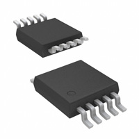
FSUSB20L10X
-40 to +85°C
10-Lead MicroPak™, 1.6 x 2.1mm
FSUSB20BQX
-40 to +85°C
14-Terminal Depopulation Quad Very-Thin Flat Pack No Lead
(DQFN), JEDEC MO-241, 2.5 X 3.0mm
-40 to +85°C
10-Lead Molded Small Outline Package (MSOP), JEDEC MO-187,
3.0mm Wide
FSUSB20MUX
©2005 Fairchild Semiconductor Corporation
FSUSB20 • Rev. 1.0.3
Packing
Method
Tape and
Reel
Tube
Tape and
Reel
www.fairchildsemi.com
FSUSB20 — Low-Power, 1-Port, High-Speed USB 2.0 (480Mbps) Switch
April 2012
�Figure 1. MicroPak™ (Top View)
Figure 2.
Figure 3. DQFN (Top Through View)
Analog Symbol
Figure 4. MSOP (Top Through View)
Pin Descriptions
Pin # MicroPak™ / MSOP
Pin # DQFN
Pin Names
Description
1
2
S
Select Input
2, 3, 7, 8
3, 5, 10, 12
1B1, 1B2, 2B2, 2B1
Bus B
5
7
GND
Ground
4, 6
6, 9
1A, 2A
Bus A
9
12
OE
Bus Switch Enable
10
14
VCC
Supply Voltage
FSUSB20 — Low-Power, 1-Port, High-Speed USB 2.0 (480Mbps) Switch
Connection Diagrams
Truth Table
S
OE
Function
Don’t Care
HIGH
Disconnect
LOW
LOW
A=B1
HIGH
LOW
A=B2
© 2005 Fairchild Semiconductor Corporation
FSUSB20 • Rev. 1.0.3
www.fairchildsemi.com
2
�Stresses exceeding the absolute maximum ratings may damage the device. The device may not function or be
operable above the recommended operating conditions and stressing the parts to these levels is not recommended.
In addition, extended exposure to stresses above the recommended operating conditions may affect device reliability.
The absolute maximum ratings are stress ratings only.
Symbol
Parameter
Min.
Max.
Unit
-0.5
4.6
V
VCC
Supply Voltage
VS
DC Switch Voltage
-0.5
VCC + 0.05
V
VIN
(1)
DC Input Voltage
-0.5
4.6
V
IIK
DC Input Diode Current, VIN