Is Now Part of
To learn more about ON Semiconductor, please visit our website at
www.onsemi.com
ON Semiconductor and the ON Semiconductor logo are trademarks of Semiconductor Components Industries, LLC dba ON Semiconductor or its subsidiaries in the United States and/or other countries. ON Semiconductor owns the rights to a number
of patents, trademarks, copyrights, trade secrets, and other intellectual property. A listing of ON Semiconductor’s product/patent coverage may be accessed at www.onsemi.com/site/pdf/Patent-Marking.pdf. ON Semiconductor reserves the right
to make changes without further notice to any products herein. ON Semiconductor makes no warranty, representation or guarantee regarding the suitability of its products for any particular purpose, nor does ON Semiconductor assume any liability
arising out of the application or use of any product or circuit, and specifically disclaims any and all liability, including without limitation special, consequential or incidental damages. Buyer is responsible for its products and applications using ON
Semiconductor products, including compliance with all laws, regulations and safety requirements or standards, regardless of any support or applications information provided by ON Semiconductor. “Typical” parameters which may be provided in ON
Semiconductor data sheets and/or specifications can and do vary in different applications and actual performance may vary over time. All operating parameters, including “Typicals” must be validated for each customer application by customer’s
technical experts. ON Semiconductor does not convey any license under its patent rights nor the rights of others. ON Semiconductor products are not designed, intended, or authorized for use as a critical component in life support systems or any FDA
Class 3 medical devices or medical devices with a same or similar classification in a foreign jurisdiction or any devices intended for implantation in the human body. Should Buyer purchase or use ON Semiconductor products for any such unintended
or unauthorized application, Buyer shall indemnify and hold ON Semiconductor and its officers, employees, subsidiaries, affiliates, and distributors harmless against all claims, costs, damages, and expenses, and reasonable attorney fees arising out
of, directly or indirectly, any claim of personal injury or death associated with such unintended or unauthorized use, even if such claim alleges that ON Semiconductor was negligent regarding the design or manufacture of the part. ON Semiconductor
is an Equal Opportunity/Affirmative Action Employer. This literature is subject to all applicable copyright laws and is not for resale in any manner.
�FSUSB30
低功率、双端口、高速 USB2.0(480Mbps) 开关
特性
?
?
?
?
?
?
?
说明
低导通电容:3.7pF (典型值)
低导通电阻:6.5W (典型值)
低功耗:1μA (最大值)
衆 t10μA 最大 ICCT 超过扩展控制电压范围
(VIN = 2.6V, VCC = 4.3V)
宽 -3dB 带宽, >720MHz
8kV 静电放电保护
当 VCC = 0V; D+/ D- 引脚可耐受的电压达到 5.5V 时,
会提供断电保护
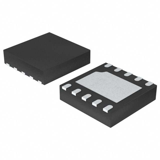
封装:
衆 t10 引脚 MicroPak™ (1.6 x 2.1mm)
衆 t10 引脚 MSOP
衆 t10 引脚 UMLP (1.4 x 1.8mm)
应用
?
FSUSB30 是一款低功率、 2 端口、高速 USB 2.0 开关。
该器件配置为双刀双掷 (DPDT) 开关,专为在两个高速
(480Mbps) 源或高速和全速 (12Mbps) 源之间切换进行了
优化。 FSUSB30 符合 USB2.0 的要求,并且具有 3.7pF
的极低导通电容 (CON)。此器件的宽带宽 (720MHz) 超过
了通过三次谐波所需的带宽,这使得信号的边沿和相位失
真降到最小。出色的通道间串扰性能可实现最小的干扰。
FSUSB30 在 D+ / D- 引脚上包含了特殊的电路,在断电时
可使器件承受过压条件。同时,当应用于 S 引脚的控制电
压小于电源电压 (VCC) 时,该器件可以最大限度地降低功
耗。此特性对超便携式应用 (例如手机)尤为重要,可支
持基带处理器通用 I/O 的直接接口。其他应用包括便携手
机、PDA、数码相机、打印机和笔记本电脑中共享的开关
和连接器。
手机、个人数字处理 (PDA)、数码相机和笔记本 LCD
显示器、电视机和机顶盒
相关应用说明
?
AN-6022 使用 FSUSB30/FSUSB31,以符合 USB 2.0
故障条件要求
订购信息
封装编号
产品代码记号
FSUSB30L10X
订货号
MAC010A
FJ
FSUSB30MUX
MUA10A
FSUSB30
FSUSB30UMX
MLP010A
GJ
封装说明
10 引脚 MicroPak, 1.6 x 2.1mm
10 引脚模塑小外形封装 (MSOP), JEDEC MO-187, 3.0mm 宽
10 引脚方形超薄 MLP (UMLP) 1.4 x 1.8mm
1D+
USB2.0
Controller
Set Top Box
(STB) CPU
or
DSP
Processor
VCC
FSUSB30
D+
1D–
USB
Connector
D–
2D+
DVR or
Mass Storage
2D–
Controller
.
Control
S
OE
图 1. 典型应用
MicroPak 是飞兆半导体公司的商标。
© 2006 飞兆半导体公司
FSUSB30 Rev. 1.1.8
www.fairchildsemi.com
FSUSB30 — 低功率、双端口、高速 USB2.0(480Mbps) 开关
2013 年 3 月
�模拟符号
OE
HSD1–
HSD2–
D–
Pad Assignments for MicroPak
9
8
7
6
HSD1+
D+
HSD2+
HSD1–
D–
VCC
10
GND
5
3
S
4
HSD2+
HSD1+
S
2
OE
D+
1
HSD2–
(Top View)
引脚描述
引脚名
说明
OE
总线开关使能
S
选择输入
D+, D-, HSDn+, HSDn-
数据端口
NC
未连接
Pad Assignments for DQFN
NC
VCC
1
14
S
2
13
OE
HSD1+
3
12
HSD1–
NC
4
11
NC
HSD2+
5
10
HSD2–
D+
6
9
D–
7
真值表
8
GND NC
(Top Through View)
Pin Assignment for MSOP
1
10
VCC
HSD1+
2
9
OE
HSD2+
3
8
HSD1–
D+
4
7
HSD2–
GND
5
6
D–
S
Control
S
OE
功能
X
高
未连接
低
低
D+, D- = HSD1n
高
低
D+, D- = HSD2n
(Top Through View)
9
Sel
10
HSD2–
VCC
7
6
1
2
HSD1+
8
HSD2+
OE
HSD1–
Pad Assignments for µMLP
5
D–
4
GND
3
D+
(Top Through View)
© 2006 飞兆半导体公司
FSUSB30 Rev. 1.1.8
www.fairchildsemi.com
2
FSUSB30 — 低功率、双端口、高速 USB2.0(480Mbps) 开关
连接图
�应力超过绝对最大额定值,可能会损坏设备。在超出推荐的工作条件的情况下,该器件可能无法正常运行或操作,且不
建议让器件在这些条件下长期工作。此外,过度暴露在高于推荐的工作条件下,会影响器件的可靠性。绝对最大额定值
仅是额定应力值。
符号
VCC
VCNTRL
VSW
IIK
参数
最低
最大值
单位
-0.5
+5.5
V
电源电压
DC 输入电压
(1)
直流开关 I/O 电压 (1)
-0.5
VCC
V
HSDnX
0.5
VCC
V
D+,D- 考虑到 VCC > 0
0.5
VCC
V
D+,D- 考虑到 VCC = 0
-0.50
VCC
V
直流输入二极管电流
IOUT
直流输出电流
TSTG
存储温度
ESD
人体模型
-50
mA
50
mA
+150
°C
全部引脚
8
kV
输入 / 输出至地
8
kV
-65
注意:
1. 当观测输入与输出二极管电流额定值时,该输入与输出可能超出负额定值。
推荐工作条件
推荐的操作条件表定义了器件的真实工作条件。指定推荐的工作条件,以确保设备的最佳性能达到数据表中的规格。飞
兆半导体建议不要超过推荐工作条件,也不能按照绝对最大额定值进行设计。
符号
参数
最低
最大值
单位
3.0
4.3
V
控制输入电压
0
VCC
V
开关输入电压
0
VCC
V
-40
+85
°C
250
°C/W
VCC
电源电压
VIN
VSW
TA
JA
工作温度
热阻, 10 MicroPak
注意:
2. 控制输入必须保持高电平或低电平,不允许浮动。
© 2006 飞兆半导体公司
FSUSB30 Rev. 1.1.8
www.fairchildsemi.com
3
FSUSB30 — 低功率、双端口、高速 USB2.0(480Mbps) 开关
绝对最大额定值
�若无其他说明,所有典型值都在 25°C 下测得。
符号
参数
VIK
箝位二极管电压
VIH
输入电压高电平
VIL
输入电压低电平
IIN
控制脚输入漏电流
IOZ
关断漏电流
IOFF
电源关断漏
电流 (D+, D–)
RON
开关导通电阻 (3)
∆RON
Delta
工作条件
VCC (V)
IIN = -18mA
TA = -40°C 至 +85°C
最小值 典型值 最大值
3.0
-1.2
V
3.0 至 3.6
1.3
V
4.3
1.7
V
3.0 至 3.6
0.5
4.3
RON(4)
单位
V
0.7
V
VSW = 0.0V 至 VCC
4.3
-1.0
1.0
µA
0 ≤ Dn, HSD1n, HSD2n ≤ VCC
4.3
-2.0
2.0
µA
VSW = 0V 至 4.3V, VCC = 0V
0
-2.0
2.0
µA
10.0
7.0
VSW = 0.4V, ION = -8mA
3.0
6.5
VSW = 0V, IO = 30mA, 25°C
3.6
VSW = 0.4V, ION = -8mA
3.0
0.35
2.0
RON 平坦度
RON 平坦度 (3)
VSW = 0.0V - 1.0V,
ION = -8mA
3.0
ICC
静态电源电流
VCNTRL = 0.0V 或 VCC,
IOUT = 0
4.3
1.0
µA
ICCT
每个控制电压的 ICC 电
流增量
VCNTRL (控制输入) = 2.6V
4.3
10.0
µA
单位
图位
说明:
3. 在通过开关的指定电流下,由 Dn、 HSD1n 和 HSD2n 引脚之间的电压降测得。
导通电阻决定于这两个端口上的电压降。
4. 由产品特性保证。
交流电气特性
若无其他说明,所有典型值都在 25°C, Vcc=3.3V 时测得。
符号
参数
工作条件
VCC (V)
TA = -40°C 至 +85°C
最小值 典型值
最大值
tON
导通时间 S,
OE 至 Output
HD1n, HD2n = 0.8V,
RL = 50, CL = 5pF
3.0 至 3.6
13
30
ns
图9
tOFF
关断时间 S,
OE 至 Output
HD1n, HD2n = 0.8V,
RL = 50, CL = 5pF
3.0 至 3.6
12
25
ns
图9
tPD
传输延迟 (4)
RL = 50, CL = 5pF
3.3
0.25
ns
图7
图8
tBBM
先开后合
RL = 50, CL = 5pF,
VIN = 0.8V
3.0 至 3.6
ns
图 10
OIRR
关断隔离 (非相邻)
f = 240MHz, RT = 50
3.0 至 3.6
-30
dB
图 13
Xtalk
非相邻通道串扰
RT = 50, f = 240MHz
3.0 至 3.6
-45
dB
图 14
MHz
图 12
BW
-3dB 带宽
© 2006 飞兆半导体公司
FSUSB30 Rev. 1.1.8
RT = 50, CL = 0pF
3.0 至 3.6
RT = 50, CL = 5pF
2.0
6.5
720
550
www.fairchildsemi.com
4
FSUSB30 — 低功率、双端口、高速 USB2.0(480Mbps) 开关
直流电气特性
�符号
参数
工作条件
VCC (V)
TA = -40°C 至 +85°C
最小值 典型值 最大值
单位
图位
tSK(O)
通道间相位差 (5)
RL = 50, CL = 5pF
3.0 至 3.6
50
ps
图7
图 11
tSK(P)
在相同输出下,反向
转换的时滞 (5)
RL = 50, CL = 5pF
3.0 至 3.6
20
ps
图7
图 11
总抖动 (5)
RL = 50, CL = 5pF,
480 Mbps 时,tR = tF = 500ps 3.0 至 3.6
(PRBS = 215 - 1)
200
ps
tJ
注意:
5. 由产品特性保证。
电容值
符号
参数
工作条件
TA = -40°C 至 +85°C
最小值 典型值 最大值
单位
图位
pF
图 16
CIN
控制引脚输入电容
VCC = 0V
CON
D1n, D2n, Dn 导通电容
VCC = 3.3, OE = 0V
3.7
pF
图 15
COFF
D1n, D2n 关断电容
VCC 和 OE = 3.3
2.5
pF
图 16
© 2006 飞兆半导体公司
FSUSB30 Rev. 1.1.8
1.5
www.fairchildsemi.com
5
FSUSB30 — 低功率、双端口、高速 USB2.0(480Mbps) 开关
高速 USB 相关的交流电气特性
�FSUSB30 — 低功率、双端口、高速 USB2.0(480Mbps) 开关
典型特性
Frequency Response
0
-1
Gain (dB)
-2
-3
-4
-5
-6
-7
-8
1
10
100
1000
10000
CL = 0pF, VCC = 3.3V
Frequency (MHz)
图 2. 增益 vs. 频率
Off Isolation (dB)
Frequency Response
0
-10
-20
-30
-40
-50
-60
-70
-80
-90
-100
-110
-120
1
10
100
1000
Frequency (MHz)
图 3. 关断隔离
Crosstalk (dB)
Frequency Response
0
-10
-20
-30
-40
-50
-60
-70
-80
-90
-100
-110
-120
1
10
100
Frequency (MHz)
1000
VCC = 3.3V
图 4. 串扰
© 2006 飞兆半导体公司
FSUSB30 Rev. 1.1.8
www.fairchildsemi.com
6
�VON
IDn(OFF)
NC
A
HSDn
Dn
VIN
VIN
ION
Select
GND
Select
GND
VS = 0 or VCC
GND
VS = 0 to VCC
Each switch port is tested separately.
RON = VON / ION
图 5. 导通电阻
图 6. 关断漏电流
D+, D–
800mV
Input: HSDn+,
HSDn–
400mV
VIN
RS
GND
tFALL = 500ps
tRISE = 500ps
HSDn
RL VOUT
CL
GND
VSel
90%
90%
50%
50%
10%
10%
VOH
GND
Output: D+, D–
RL, RS, and CL are functions of the application environment
(see AC Electrical tables for specific values).
50%
50%
VOL
tPLH
CL includes test fixture and stray capacitance.
图 7. 交流测试电路负载
tPHL
图 8. 开关传输延迟波形
tFALL = 2.5ns
tRISE = 2.5ns
VCC
90%
Input – S, OE
VCC/2
GND
90%
VCC/2
10%
10%
VOH
90%
90%
Output – VOUT
VOL
tON
tOFF
图 9. 开通 / 关断波形
© 2006 飞兆半导体公司
FSUSB30 Rev. 1.1.8
www.fairchildsemi.com
7
FSUSB30 — 低功率、双端口、高速 USB2.0(480Mbps) 开关
测试框图
�VCC
HSDn
VO
VOUT
D+, D–
RL
VCC
Control
Input
HSDn
CL*
50%
0V
tR = tF = 2.5ns (10–90%)
S
Control
Input
VOUT
GND
0.9 x VOUT
tD
*CL includes test fixture and stray capacitance.
图 10. “ 先开后合 ”(tBBM)
tFALL = 500ps
tRISE = 500ps
800mV
90%
Input: D+, D–
50%
10%
400mV
10%
tFALL = 500ps
tRISE = 500ps
800mV
90%
Input: HSDn+
HSDn–
50%
VOH
Output1: HSD1+
HSD1–
90%
50%
10%
400mV
90%
50%
50%
50%
VOL
10%
VOH
tPLH1
tPHL1
50%
50%
VOH
50%
Output: D+, D–
50%
Output1: D2+, D2–
VOL
VOL
tPLH
tPHL
tPLH2
TSK(P) = | tPHL – tPLH |
Pulse Skew, TSK(P)
tPHL2
TSK(O) = | tPLH1 – tPLH2 | or | tPHL1 – tPHL2 |
Output Skew, TSK(OUT)
图 11. 开关时滞测试
Network Analyzer
FSUSB30
RS
VIN
VS
GND
GND
VSel
GND
VOUT
GND
RS and RT are functions of the application environment
(See AC Electrical Tables for specific values).
RT
GND
图 12. 带宽
© 2006 飞兆半导体公司
FSUSB30 Rev. 1.1.8
www.fairchildsemi.com
8
FSUSB30 — 低功率、双端口、高速 USB2.0(480Mbps) 开关
VCC
�FSUSB30 — 低功率、双端口、高速 USB2.0(480Mbps) 开关
Network Analyzer
FSUSB30
RS
VIN
VS
GND
RT
GND
VSel
GND
GND
VOUT
RT
GND
OFF-Isolation = 20 Log (VOUT / VIN)
GND
图 13. 通道的关断隔离
NC
Network Analyzer
FSUSB30
RS
VIN
VS
GND
GND
VSel
RT
GND
GND
GND
RS and RT are functions of the application environment
(50, 75 or 100Ω)
RT
VOUT
GND
Crosstalk = 20 Log (VOUT / VIN)
图 14. 非相邻通道间串扰
Capacitance
Meter
Dn
FSUSB30
Dn
S
S
Capacitance
Meter
VSel = 0 or VCC
f = 240MHz
f = 240MHz
D1n, D2n
图 15. 通道导通电容
© 2006 飞兆半导体公司
FSUSB30 Rev. 1.1.8
FSUSB30
VSel = 0 or VCC
D1n, D2n
图 16. 通道关断电容
www.fairchildsemi.com
9
�上电保护
在 USB 2.0 规范的第 7.1.1 节,说明了 USB 设备必须能
够耐受关闭或开启 USB 设备时 Vbus 与 D+ 或 D- 的短
路。 FSUSB30 配置可有效满足这两项要求。
USB 2.0 规范还说明, USB 设备应该能够耐受传输数据
时出现的 Vbus 短路。为了提供针对这种情况的防护,飞
兆建议在开关 VCC 引脚和电源电压轨之间加入一个
100W 串行电阻。在出现过压时,这种更改操作可以限制
流回 VCC 轨道的电流,从而将电流保持在安全工作范围
内。在这种应用中,开关将完整的 5.25V 输入信号通过选
择的输出口发送出去,同时维持未被选择的引脚上的关断
隔离。
断电保护
对于 Vbus 短路,开关需要能够耐受这种情况至少 24 小
时。 FSUSB30 具有专门设计的电路,可以防止关闭电源
和过压条件下的意外信号泄漏,并且保证系统可靠性。这
种保护也被增加到普通引脚 (D+, D-)。
VCC= 3.6 V
100 Ohms
HSD+
HSD+
HSD-
D+ = 5.25V
FSUSB30
HSD-
D- = 5.25V
Figure 17. Adding 100 resistor in series with the VCC supply allows the FSUSB30 to withstand a
Vbus short when powered up
For more information, see Applications Note AN-6022 Using the FSUSB30 to Comply with USB 2.0 Fault
Condition Requirements at www.fairchildsemi.com
© 2006 飞兆半导体公司
FSUSB30 Rev. 1.1.8
www.fairchildsemi.com
10
FSUSB30 — 低功率、双端口、高速 USB2.0(480Mbps) 开关
应用指南:符合 USB 2.0 Vbus 短路要求
�DQFN 的卷带形式
封装指示符
BQX
带第 节
位腔
空白段 (始点终点)
载体
空白片尾 (插孔末端)
腔状态
盖带状态
125 (典型值)
空
密封
2500/3000
装满
密封
75 (典型值)
空
密封
卷带尺寸
尺寸以英寸 (毫米)表示,除非另有说明。
© 2006 飞兆半导体公司
FSUSB30 Rev. 1.1.8
www.fairchildsemi.com
11
FSUSB30 — 低功率、双端口、高速 USB2.0(480Mbps) 开关
卷带和卷盘规格
�尺寸以英寸 (毫米)表示,除非另有说明。
卷带大小
A
B
C
D
N
W1
W2
(12mm)
13.0
(330)
0.059
(1.50)
0.512
(13.00)
0.795
(20.20)
7.008
(178)
0.488
(12.4)
0.724
(18.4)
© 2006 飞兆半导体公司
FSUSB30 Rev. 1.1.8
www.fairchildsemi.com
12
FSUSB30 — 低功率、双端口、高速 USB2.0(480Mbps) 开关
DQFN 的卷带尺寸
�FSUSB30 — 低功率、双端口、高速 USB2.0(480Mbps) 开关
MSOP 的卷带尺寸
尺寸以英寸 (毫米)表示,除非另有说明。
MSOP 的卷带尺寸
尺寸以英寸 (毫米)表示,除非另有说明。
卷带大小
A
B
C
D
N
W1
W2
W3
(12mm)
13
(330)
0.059
(1.5)
0.512
(13)
0.795
(20.2)
7.008
(178)
0.448
(12.4)
0.724
(18.4)
0.468-0.606
(11.9 -15.4)
© 2006 飞兆半导体公司
FSUSB30 Rev. 1.1.8
www.fairchildsemi.com
13
�0.10 C
2.10
2X
A
1.62
B
KEEPOUT ZONE, NO TRACES
OR VIAS ALLOWED
(0.11)
1.12
1.60
PIN1 IDENT IS
2X LONGER THAN
OTHER LINES
0.56
0.10 C
2X
TOP VIEW
(0.35) 10X
(0.25) 10X
0.50
RECOMMENDED LAND PATTERN
0.55 MAX
0.05 C
0.05 C
0.05
0.00
C
(0.20)
0.35
0.25
SIDE VIEW
D
0.65
0.55
DETAIL A
0.35
0.25
1
4
0.35
0.25
DETAIL A 2X SCALE
0.56
10
(0.29)
(0.15)
(0.36)
5
6
9
0.50
0.25 9X
0.15
1.62
0.35 9X
0.25
0.10
0.05
C A B
C
ALL FEATURES
BOTTOM VIEW
NOTES:
A. PACKAGE CONFORMS TO JEDEC
REGISTRATION MO-255, VARIATION UABD .
B. DIMENSIONS ARE IN MILLIMETERS.
C. DIMENSIONS AND TOLERANCES PER
ASME Y14.5M, 1994.
D. PRESENCE OF CENTER PAD IS PACKAGE
SUPPLIER DEPENDENT. IF PRESENT IT
IS NOT INTENDED TO BE SOLDERED AND
HAS A BLACK OXIDE FINISH.
E. DRAWING FILENAME: MKT-MAC10Arev5.
图 17. 10 引脚 MicroPak, 1.6 x 2.1mm
要了解卷带和卷盘规格,请访问飞兆半导体的网站:http://www.fairchildsemi.com/products/logic/pdf/micropak_tr.pdf.
封装图纸是作为一项服务而提供给考虑选用飞兆半导体产品的客户。具体参数可进行改动,且无需做出相应通知。请注意图纸上的版本
和 / 或日期,并联系飞兆半导体代表核实或获得最新版本。封装规格并不超出飞兆公司全球范围内的条款与条件,尤其指保修,保修涉
及飞兆半导体的全部产品。
请经常访问飞兆半导体在线封装网页,以获取最新封装图纸。
http://www.fairchildsemi.com/packaging/.
© 2006 飞兆半导体公司
FSUSB30 Rev. 1.1.8
www.fairchildsemi.com
14
FSUSB30 — 低功率、双端口、高速 USB2.0(480Mbps) 开关
物理尺寸测试
�FSUSB30 — 低功率、双端口、高速 USB2.0(480Mbps) 开关
物理尺寸测试
图 18. 10 引脚模塑小外形封装 (MSOP), JEDEC MO-187, 3.0mm 宽
封装图纸是作为一项服务而提供给考虑选用飞兆半导体产品的客户。具体参数可进行改动,且无需做出相应通知。请注意图纸上的版本和
/ 或日期,并联系飞兆半导体代表核实或获得最新版本。封装规格并不超出飞兆公司全球范围内的条款与条件,尤其指保修,保修涉及飞兆
半导体的全部产品。
请经常访问飞兆半导体在线封装网页,以获取最新封装图纸。
http://www.fairchildsemi.com/packaging/.
© 2006 飞兆半导体公司
FSUSB30 Rev. 1.1.8
www.fairchildsemi.com
15
�1.40
0.10 C
A
B
2X
(9X)
1.70
0.563
0.663
1.80
1
PIN#1 IDENT
2.10
0.10 C
TOP VIEW
0.40
2X
(10X) 0.225
0.55 MAX.
0.10 C
0.08 C
RECOMMENDED
LAND PATTERN
(0.15)
SEATING C
PLANE
0.05
0.00
0.55
SIDE VIEW
1.85
(10X) 0.225
6
OPTIONAL MINIMIAL
TOE LAND PATTERN
0.40
1
NOTES:
PIN#1 IDENT
A. PACKAGE DOES NOT CONFORM TO
ANY JEDEC STANDARD.
B. DIMENSIONS ARE IN MILLIMETERS.
0.15
(10X)
0.25
10
BOTTOM VIEW
0.10 C A B
0.05 C
C. DIMENSIONS AND TOLERANCES PER
ASME Y14.5M, 1994.
D. LAND PATTERN RECOMMENDATION IS
BASED ON FSC DESIGN ONLY.
0.55
0.45
0.25
0.15
9X
0.45
0.40
0.35
(9X)
0.45
3
DETAIL A
1.45
PACKAGE
EDGE
45°
DETAIL A
SCALE : 2X
F. FAIRCHILD SEMICONDUCTOR.
LEAD
OPTION 2
LEAD
OPTION 1
SCALE : 2X
E. DRAWING FILENAME: MKT-UMLP10Arev5.
SCALE : 2X
图 19. 10 引脚,方形,超薄膜塑无铅封装 (UMLP), 1.4 x 1.8mm
封装图纸是作为一项服务而提供给考虑选用飞兆半导体产品的客户。具体参数可进行改动,且无需做出相应通知。请注意图纸上的版本
和 / 或日期,并联系飞兆半导体代表核实或获得最新版本。封装规格并不超出飞兆公司全球范围内的条款与条件,尤其指保修,保修涉
及飞兆半导体的全部产品。
请经常访问飞兆半导体在线封装网页,以获取最新封装图纸。
http://www.fairchildsemi.com/packaging/.
© 2006 飞兆半导体公司
FSUSB30 Rev. 1.1.8
www.fairchildsemi.com
16
FSUSB30 — 低功率、双端口、高速 USB2.0(480Mbps) 开关
物理尺寸测试
�FSUSB30 — 低功率、双端口、高速 USB2.0(480Mbps) 开关
© 2006 飞兆半导体公司
FSUSB30 Rev. 1.1.8
www.fairchildsemi.com
17
�ON Semiconductor and
are trademarks of Semiconductor Components Industries, LLC dba ON Semiconductor or its subsidiaries in the United States and/or other countries.
ON Semiconductor owns the rights to a number of patents, trademarks, copyrights, trade secrets, and other intellectual property. A listing of ON Semiconductor’s product/patent
coverage may be accessed at www.onsemi.com/site/pdf/Patent−Marking.pdf. ON Semiconductor reserves the right to make changes without further notice to any products herein.
ON Semiconductor makes no warranty, representation or guarantee regarding the suitability of its products for any particular purpose, nor does ON Semiconductor assume any liability
arising out of the application or use of any product or circuit, and specifically disclaims any and all liability, including without limitation special, consequential or incidental damages.
Buyer is responsible for its products and applications using ON Semiconductor products, including compliance with all laws, regulations and safety requirements or standards,
regardless of any support or applications information provided by ON Semiconductor. “Typical” parameters which may be provided in ON Semiconductor data sheets and/or
specifications can and do vary in different applications and actual performance may vary over time. All operating parameters, including “Typicals” must be validated for each customer
application by customer’s technical experts. ON Semiconductor does not convey any license under its patent rights nor the rights of others. ON Semiconductor products are not
designed, intended, or authorized for use as a critical component in life support systems or any FDA Class 3 medical devices or medical devices with a same or similar classification
in a foreign jurisdiction or any devices intended for implantation in the human body. Should Buyer purchase or use ON Semiconductor products for any such unintended or unauthorized
application, Buyer shall indemnify and hold ON Semiconductor and its officers, employees, subsidiaries, affiliates, and distributors harmless against all claims, costs, damages, and
expenses, and reasonable attorney fees arising out of, directly or indirectly, any claim of personal injury or death associated with such unintended or unauthorized use, even if such
claim alleges that ON Semiconductor was negligent regarding the design or manufacture of the part. ON Semiconductor is an Equal Opportunity/Affirmative Action Employer. This
literature is subject to all applicable copyright laws and is not for resale in any manner.
PUBLICATION ORDERING INFORMATION
LITERATURE FULFILLMENT:
Literature Distribution Center for ON Semiconductor
19521 E. 32nd Pkwy, Aurora, Colorado 80011 USA
Phone: 303−675−2175 or 800−344−3860 Toll Free USA/Canada
Fax: 303−675−2176 or 800−344−3867 Toll Free USA/Canada
Email: orderlit@onsemi.com
© Semiconductor Components Industries, LLC
N. American Technical Support: 800−282−9855 Toll Free
USA/Canada
Europe, Middle East and Africa Technical Support:
Phone: 421 33 790 2910
Japan Customer Focus Center
Phone: 81−3−5817−1050
www.onsemi.com
1
ON Semiconductor Website: www.onsemi.com
Order Literature: http://www.onsemi.com/orderlit
For additional information, please contact your local
Sales Representative
www.onsemi.com
�


 工商网监
湘ICP备2023018690号
工商网监
湘ICP备2023018690号
