FSUSB46 — Hi-Speed USB2.0 (480Mbps) DPST Switch
with Dedicated Charger Port Detection
Features
Description
The FSUSB46 is a bi-directional, low-power, Hi-Speed,
USB2.0 switch. Configured as a double-pole, singlethrow switch (DPST) switch, it is optimized for switching
a Hi-Speed (480Mbps) source.
Low On Capacitance: 7.0pF Typical
Low On Resistance: 3.9Ω Typical
Low Power Consumption: 1μA Maximum
- 15μA Maximum ICCT over an Expanded Voltage
Range (VIN=1.8V, VCC=4.3V)
Wide -3db Bandwidth: > 720MHz
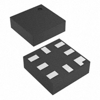
Packaged in Pb-free, 8-Lead MicroPak™ (1.6mm
wide), US8 (3.1mm wide), and UMLP (1.4x1.4mm)
8kV ESD Rating, >16kV Power/GND ESD Rating
Power-Off Protection on All Ports When VCC=0V
- D+/D- Pins Tolerate up to 5.25V
Applications
Cell phone, PDA, Digital Camera, and Notebook
LCD Monitor, TV, and Set-Top Box
IMPORTANT NOTE:
For additional performance information, please contact
analogswitch@fairchildsemi.com.
The FSUSB46 is compatible with the requirements of
USB2.0 and features an extremely low on capacitance
(CON) of 3.9pF. The wide bandwidth of this device
(720MHz) exceeds the bandwidth needed to pass the
third harmonic, resulting in signals with minimum edge
and phase distortion. Superior channel-to-channel
crosstalk also minimizes interference.
The FSUSB46 contains special circuitry on the switch
I/O pins for applications where the VCC supply is
powered-off (VCC=0), which allows the device to
withstand an over-voltage condition. This device is
designed to minimize current consumption even when
the control voltage applied to the /OE pin is lower than
the supply voltage (VCC). This feature is especially
valuable to ultra-portable applications, such as cell
phones, allowing for direct interface with the generalpurpose I/Os of the baseband processor. An additional
feature is the detection of the 1-1 (high/high) state on
D+/D- to signal an interrupt (INT) to the processor when
entering a dedicated charging port mode of operation.
Ordering Information
Part Number
Operating
Temperature Range
FSUSB46L8X
FSUSB46K8X
-40 to +85°C
-40 to +85°C
FSUSB46UMX
-40 to +85°C
Package
8-Lead MicroPak™ 1.6mm Wide
8-Lead US8, JEDEC MO187, Variation CA 3.1mm
8-Lead Ultrathin Molded Leadless Package (UMLP),
1.2 x 1.4mm
Eco Status
RoHS
Green
Green
For Fairchild’s definition of Eco Status, please visit: http://www.fairchildsemi.com/company/green/rohs_green.html.
MicroPak™ is a trademark of Fairchild Semiconductor Corporation.
INT
D+
HSD+
DHSD/OE
Figure 1. Analog Symbol
© 2007 Fairchild Semiconductor Corporation
FSUSB46 • Rev. 1.0.4
www.fairchildsemi.com
FSUSB46 — Hi-Speed USB2.0 (480Mbps) DPST Switch with Dedicated Charger Port Detection
March 2013
�2
D+
3
4
6
HSD-
5
D-
1
8
Vcc
HSD-
2
3
7
6
5
HSD+
D+
DGND
GND
Figure 2. MicroPak™
(Top Through View)
VCC
INT
4
/OE
HSD–
D–
INT
8
7
6
1
2
Figure 3. US8
(Top Through View)
GND
5
3
4
D+
HSD+
7
HSD+
8
1
/OE
/OE
INT
Vcc
Figure 4. UMLP
(Top Through View)
Pin Definitions
Pin Name
Description
INT
Interrupt Signaling Output Pin
/OE
Switch Enable
D+, D-
USB Data Bus Connector
HSD+, HSD-
USB Source Inputs
GND
Ground
VCC
Supply Voltage
Truth Table
Data Path
/OE
Charger Detect Path
Switch Connection
D+ D-
INT Output
HIGH
D+, D- = Open
1-1
LOW
LOW
D+, D- = HSD+, HSD-
0X, X0
HIGH
© 2007 Fairchild Semiconductor Corporation
FSUSB46 • Rev. 1.0.4
FSUSB46 — Hi-Speed USB2.0 (480Mbps) DPST Switch with Dedicated Charger Port Detection
Pin Configurations
www.fairchildsemi.com
2
�Stresses exceeding the absolute maximum ratings may damage the device. The device may not function or be
operable above the recommended operating conditions and stressing the parts to these levels is not recommended.
In addition, extended exposure to stresses above the recommended operating conditions may affect device reliability.
The absolute maximum ratings are stress ratings only.
Symbol
VCC
VCNTRL
Parameter
Supply Voltage
(1)
DC Input Voltage (S)
(1)
Min.
Max.
Unit
-0.5
+5.5
V
-0.5
VCC
V
5.25
VSW
DC Switch I/O Voltage
-0.50
IIK
DC Input Diode Current
-50
IOUT
DC Output Current
TSTG
Storage Temperature
ESD
-65
Human Body Model, JEDEC: JESD22-A114
50
mA
+150
°C
All Pins
7
I/O to GND
8
Power to GND
16
Charged Device Model, JEDEC: JESD22-C101
V
mA
kV
2
Note:
1. The input and output negative ratings may be exceeded if the input and output diode current ratings are observed.
Recommended Operating Conditions
The Recommended Operating Conditions table defines the conditions for actual device operation. Recommended
operating conditions are specified to ensure optimal performance to the datasheet specifications. Fairchild does not
recommend exceeding them or designing to Absolute Maximum Ratings.
Symbol
VCC
VCNTRL
VSW
TA
Parameter
Supply Voltage
Control Input Voltage (/OE)
(2)
Min.
Max.
Unit
3.0
4.3
V
0
VCC
V
Switch I/O Voltage
-0.5
VCC
V
Operating Temperature
-40
+85
°C
Note:
2. The control input must be held HIGH or LOW; it must not float.
© 2007 Fairchild Semiconductor Corporation
FSUSB46 • Rev. 1.0.4
FSUSB46 — Hi-Speed USB2.0 (480Mbps) DPST Switch with Dedicated Charger Port Detection
Absolute Maximum Ratings
www.fairchildsemi.com
3
�All typical value are at 25°C, VCC=3.3V unless otherwise specified.
Symbol
Parameter
VIK
Clamp Diode Voltage
VIH
Input Voltage High
VIL
Input Voltage Low
Conditions
IIN=-18mA
VCC (V)
TA=- 40ºC to +85ºC
Min.
Typ.
3.0
Max.
-1.2
Units
V
3.0 to 3.6
1.3
V
4.3
1.7
V
3.0 to 3.6
4.3
3.0 to 3.6
2.4
4.3
2.4
0.5
V
0.7
V
VOH
Output Voltage High
IOH=-2mA
VOL
Output Voltage Low
IOL=2mA
IIN
Control Input Leakage
VSW =0 to VCC
4.3
-1
1
µA
IOZ
Off State Leakage
HSD+ or HSD-=0V, 3.6V or
floating
4.3
-2
2
µA
IOFF
Power-Off Leakage Current
(All I/O Ports)
VSW =0V to 4.3V, VCC=0V
Figure 6
0
-2
2
µA
RON
HS Switch On Resistance(3)
VSW =0.4V, ION=-8mA
Figure 5
3.0
3.9
6.5
HS Delta RON(4)
VSW =0.4V, ION=-8mA
3.0
0.65
ICC
Quiescent Supply Current
VCNTRL=0 or VCC, IOUT=0
4.3
1
µA
Increase in ICC Current Per
Control Voltage and VCC
VCNTRL=2.6V VCC=4.3V
4.3
10
µA
ICCT
VCNTRL=1.8V VCC=4.3V
4.3
20
µA
∆RON
V
3.0 to 3.6
0.25
4.3
0.25
Notes:
3. Measured by the voltage drop between HSDn and Dn pins at the indicated current through the switch.
On resistance is determined by the lower of the voltage on the two (HSDn or Dn ports).
4. Guaranteed by characterization.
© 2007 Fairchild Semiconductor Corporation
FSUSB46 • Rev. 1.0.4
V
FSUSB46 — Hi-Speed USB2.0 (480Mbps) DPST Switch with Dedicated Charger Port Detection
DC Electrical Characteristics
www.fairchildsemi.com
4
�All typical value are for VCC=3.3V at 25°C unless otherwise specified.
Symbol
Parameter
tON
Turn-On Time
/OE to Output
tOFF
Turn-Off Time
/OE to Output
tPD
Propagation Delay(5)
tBBM
Break-Before-Make
VCC (V)
TA=- 40ºC to +85ºC
Min.
Typ.
Max.
Units
3.0 to 3.6
13
30
ns
3.0 to 3.6
12
25
ns
3.3
0.25
Conditions
RL=50Ω, CL=5pF
VSW =0.8V
Figure 7, Figure 8
RL=50Ω, CL=5pF
VSW=0.8V
Figure 7, Figure 8
CL=5 pF, RL=50Ω
Figure 7, Figure 9
RL=50Ω, CL=5pF
VSW1=VSW2=0.8V
Figure 13
3.0 to 3.6
2.0
ns
6.5
ns
INT Propagation Delay(5)
RL=500Ω, CL=5pF
3.0 to 3.6
10
ns
OIRR
Off Isolation
RL=50Ω, f=240MHz
Figure 15
3.0 to 3.6
-30
dB
Xtalk
Non-Adjacent Channel
Crosstalk
RL=50Ω, f=240MHz
Figure 16
3.0 to 3.6
-45
dB
720
MHz
-3db Bandwidth
RL=50Ω, CL=0pF
Figure 14
RL=50Ω, CL=5pF
Figure 14
3.0 to 3.6
550
MHz
tPLH/HL
BW
Note:
5. Guaranteed by characterization.
USB Hi-Speed-Related AC Electrical Characteristics
Symbol
tSK(P)
tJ
Parameter
Conditions
VCC (V)
TA=- 40ºC to +85ºC
Min.
Typ.
Max.
Units
Skew of Opposite
Transitions of the Same
Output(6)
CL=5pF, RL=50Ω
Figure 10
3.0 to 3.6
20
ps
Total Jitter(6)
RL=50Ω, CL=5pf,
tR=tF=500ps (10-90%) at
480Mbps (PRBS=215 – 1)
3.0 to 3.6
200
ps
Note:
6. Guaranteed by characterization.
FSUSB46 — Hi-Speed USB2.0 (480Mbps) DPST Switch with Dedicated Charger Port Detection
AC Electrical Characteristics
Capacitance
Symbol
CIN
Parameter
Conditions
TA=- 40ºC to +85ºC
Min.
Typ. Max.
Units
Control Pin Input Capacitance
VCC=0V
1.5
pF
COUT
INT Pin Output Capacitance
VCC=0V
2.5
pF
CON
D+, D- On Capacitance
VCC=3.3V, f=1MHz
Figure 12
7.0
COFF
D+, D- Off Capacitance
VCC=3.3V
Figure 11
2.0
© 2007 Fairchild Semiconductor Corporation
FSUSB46 • Rev. 1.0.4
7.9
pF
pF
www.fairchildsemi.com
5
�VON
HSDn
D+, D-
HSDn
A
Dn
VSW
VSW
I ON
GND
/OE
V O
= VO / ION
RO
N
/OE
GND
0 or VCC
=0 o Vcc
E
N
Figure 5. On Resistance
Figure 6. Off/On Leakage
tR ISE = 2.5ns
HSDn
tFALL = 2.5ns
Dn
VCC
VS W
CL
GND RS
RL
V OUT
90%
Input – V/O E
VCC /2
VCC /2
10%
GND
GND
90%
10%
VOH
VS e l
90%
90%
Output - VO U T
GND
VO L
RL , RS , and C L are functions of the application
environment (see AC Tables for specific values)
CL includes test fixture and stray capacitance.
Figure 7. AC Test Circuit Load
tO N
tO F F
Figure 8. Turn-On / Turn-Off Waveforms
tRISE = 500ps
tFALL = 500ps
+400mV
90%
0V
- 400mV
10%
90%
10%
Output
t PHL
Figure 9. Propagation Delay (tRtF – 500ps)
Figure 10. Intra-Pair Skew Test tSK(P)
HSDn
Capacitance
Meter
/OE
Capacitance
Meter
t PLH
FSUSB46 — Hi-Speed USB2.0 (480Mbps) DPST Switch with Dedicated Charger Port Detection
Test Diagrams
HSDn
/OE
0 or Vcc
V /O =0 or Vcc
E
HSDn
HSDn
Figure 11. Channel Off Capacitance
© 2007 Fairchild Semiconductor Corporation
FSUSB46 • Rev. 1.0.4
Figure 12. Channel On Capacitance
www.fairchildsemi.com
6
�tRISE = 2.5ns
VCC
HSDn
VSW1
10%
0V
CL
GND
90%
VCC /2
Input - V/OE
Dn
RL
VOUT
GND
0.9* VOUT
0.9* VOUT
RS
tBBM
V/OE
RL, RS, and CL are functions of the application
environment (see AC Table for specific values).
CL includes text ficture and stray capacitance.
GND
Figure 13. Break-Before-Make Interval Timing
Network Analyzer
RS
GND
VIN
VS
GND
V/OE
GND
RT
GND
VOUT
GND
RS, and RT are functions of the application
environment (see AC Table for specific values).
Figure 14. Bandwidth
Network Analyzer
RS
VIN
VS
GND
V/OE
VOUT
GND
GND
RT
RS, and RT are functions of the application
environment (see AC Table for specific values).
GND
Off Isolation = 20 Log (VOUT / VIN)
Figure 15. Channel Off Isolation
Network Analyzer
RS
NC
GND
V/OE
GND
V/OE
FSUSB46 — Hi-Speed USB2.0 (480Mbps) DPST Switch with Dedicated Charger Port Detection
Test Diagrams (Continued)
VS
VIN
GND
RT
GND
RT
GND
RS, and RT are functions of the application
environment (see AC Table for specific values).
RT
VOUT
GND
Crosstalk = 20 Log (VOUT / VIN)
Figure 16. Non-Adjacent Channel-to-Channel Crosstalk
© 2007 Fairchild Semiconductor Corporation
FSUSB46 • Rev. 1.0.4
www.fairchildsemi.com
7
�0.10
2X
C
A
1.6
B
1.6
INDEX AREA
0.10
2X
C
TOP VIEW
0.55 MAX
0.05
0.05
0.00
DETAIL A
8X(0.09)
C
8X
0.35
0.25
3X(0.2)
0.05
Recommended Landpattern
C
(0.20)
1.0
2
1
4 (0.1)
C
0.35
0.25
0.5
3
8
4
7
6
5
(0.15)
0.15 8X
0.25
0.35
0.25
0.10
0.05
C A B
C
DETAIL A
PIN #1 TERMINA L
SCALE: 2X
BOTTOM VIEW
Notes:
1. PACKAGE CONFORMS TO JEDEC MO-255 VARIATION UAAD
2. DIMENSIONS ARE IN MILLIMETERS
3. DRAWING CONFORMS TO ASME Y.14M-1994
4. PIN 1 FLAG, END OF PACKAGE OFFSE T
5. DRAWING FILE NAME: MK T-MAC08AREV4
FSUSB46 — Hi-Speed USB2.0 (480Mbps) DPST Switch with Dedicated Charger Port Detection
Physical Dimensions
MAC08AREV4
Figure 17. 8-Lead MicroPak™
Package drawings are provided as a service to customers considering Fairchild components. Drawings may change in any manner
without notice. Please note the revision and/or date on the drawing and contact a Fairchild Semiconductor representative to verify or
obtain the most recent revision. Package specifications do not expand the terms of Fairchild’s worldwide terms and conditions,
specifically the warranty therein, which covers Fairchild products.
Always visit Fairchild Semiconductor’s online packaging area for the most recent package drawings:
http://www.fairchildsemi.com/packaging/.
© 2007 Fairchild Semiconductor Corporation
FSUSB46 • Rev. 1.0.4
www.fairchildsemi.com
8
�Package
Designator
Tape Section
Cavity Number
Cavity Status
Cover Tape
Status
Leader (Start End)
125 (Typical)
Empty
Sealed
Carrier
5000
Filled
Sealed
Trailer (Hub End)
75 (Typical)
Empty
Sealed
L6X, L8X, L10X
Standard Tape and Reel Specifications
Standard tape and reel specifications for MicroPak are available at Fairchild Semiconductor’s website:
http://www.fairchildsemi.com/products/logic/pdf/micropak_tr.pdf
FSUSB46L8X_F130 Tape and Reel Specifications
10
30056
2.30 ± 0.1mm
1.78 ± 0.1mm
0.68 ± 0.1mm
8
30038
1.78 ± 0.1mm
1.78 ± 0.1mm
0.68 ± 0.1mm
6
30033
1.60 ± 0.1mm
1.15 ± 0.1mm
0.70 ± 0.1mm
© 2007 Fairchild Semiconductor Corporation
FSUSB46 • Rev. 1.0.4
FSUSB46 — Hi-Speed USB2.0 (480Mbps) DPST Switch with Dedicated Charger Port Detection
Tape and Reel Specifications
www.fairchildsemi.com
9
�-A-
1.80
5
0.70
-B-
2.3±0.1
3.1±.1
3.40
8
2.70
0.15
1.00
1.55
0.30 TYP
1
0.2 C B A
ALL LEAD TIPS
4
PIN #1 IDENT.
ALL LEAD TIPS
0.1 C
0.90 MAX
0.5 TYP
DETAIL A
0.70±0.10
0.10-0.18
-C0.10
0.00
0.17-0.27
0.50TYP
0.13
A B
C
0.4 TYP
GAGE PLANE
0.12
0°-8°
A. CONFORMS TO JEDEC REGISTRATION MO-187
B. DIMENSIONS ARE IN MILLIMETERS.
C. DIMENSIONS ARE EXCLUSIVE OF BURRS, MOLD FLASH,
AND TIE BAR EXTRUSIONS.
SEATING PLANE
DETAIL A
D. DIMENSIONS AND TOLERANCES PER ANSI Y14.5M, 1982.
MAB08AREVC
FSUSB46 — Hi-Speed USB2.0 (480Mbps) DPST Switch with Dedicated Charger Port Detection
Physical Dimensions
Figure 18. 8-Lead US8, JEDEC MO-187
For current tape and reel specifications, visit Fairchild Semiconductor’s online packaging area:
http://www.fairchildsemi.com/ms/MS/MS-522.pdf
Package drawings are provided as a service to customers considering Fairchild components. Drawings may change in any manner
without notice. Please note the revision and/or date on the drawing and contact a Fairchild Semiconductor representative to verify or
obtain the most recent revision. Package specifications do not expand the terms of Fairchild’s worldwide terms and conditions,
specifically the warranty therein, which covers Fairchild products.
Always visit Fairchild Semiconductor’s online packaging area for the most recent package drawings:
http://www.fairchildsemi.com/packaging/.
© 2007 Fairchild Semiconductor Corporation
FSUSB46 • Rev. 1.0.4
www.fairchildsemi.com
10
�2X
0.10
C
1.450
0.725
1.4
B
A
0.400
0.450
1.20
1.250
0.350 7X
0.10
2X
0.625
C
0.250 8X
TOP VIEW
0.55 MAX
0.05
C
0.05
C
SEATING
PLANE
0.025
0.00
C
0.40
2
DETAIL A
0.35 7X
0.25
4
0.10
8
PIN#1 IDENT
0.30
5
1
6
(0.2)
0.15
8X
0.25
0.10
0.05
45°
0.20
0.10
C A B
C
BOTTOM VIEW
DETAIL: A
SCALE : 2x
NOTES:
A. DOES NOT CONFORMS TO JEDEC STANDARD.
B. DIMENSIONS ARE IN MILLIMETERS.
C. DIMENSIONS AND TOLERANCES CONFORMS TO ASME Y14.5M, 1994.
D. DRAWING FILE NAME : UMLP08Arev1
FSUSB46 — Hi-Speed USB2.0 (480Mbps) DPST Switch with Dedicated Charger Port Detection
Physical Dimensions
Figure 19. 8-Lead, Ultrathin Molded Leadless Package (UMLP), 1.2 x 1.4mm
Package drawings are provided as a service to customers considering Fairchild components. Drawings may change in any manner
without notice. Please note the revision and/or date on the drawing and contact a Fairchild Semiconductor representative to verify or
obtain the most recent revision. Package specifications do not expand the terms of Fairchild’s worldwide terms and conditions,
specifically the warranty therein, which covers Fairchild products.
Always visit Fairchild Semiconductor’s online packaging area for the most recent package drawings:
http://www.fairchildsemi.com/packaging/.
© 2007 Fairchild Semiconductor Corporation
FSUSB46 • Rev. 1.0.4
www.fairchildsemi.com
11
�FSUSB46 — Hi-Speed USB2.0 (480Mbps) DPST Switch with Dedicated Charger Port Detection
© 2007 Fairchild Semiconductor Corporation
FSUSB46 • Rev. 1.0.4
www.fairchildsemi.com
12
�