Is Now Part of
To learn more about ON Semiconductor, please visit our website at
www.onsemi.com
Please note: As part of the Fairchild Semiconductor integration, some of the Fairchild orderable part numbers
will need to change in order to meet ON Semiconductor’s system requirements. Since the ON Semiconductor
product management systems do not have the ability to manage part nomenclature that utilizes an underscore
(_), the underscore (_) in the Fairchild part numbers will be changed to a dash (-). This document may contain
device numbers with an underscore (_). Please check the ON Semiconductor website to verify the updated
device numbers. The most current and up-to-date ordering information can be found at www.onsemi.com. Please
email any questions regarding the system integration to Fairchild_questions@onsemi.com.
ON Semiconductor and the ON Semiconductor logo are trademarks of Semiconductor Components Industries, LLC dba ON Semiconductor or its subsidiaries in the United States and/or other countries. ON Semiconductor owns the rights to a number
of patents, trademarks, copyrights, trade secrets, and other intellectual property. A listing of ON Semiconductor’s product/patent coverage may be accessed at www.onsemi.com/site/pdf/Patent-Marking.pdf. ON Semiconductor reserves the right
to make changes without further notice to any products herein. ON Semiconductor makes no warranty, representation or guarantee regarding the suitability of its products for any particular purpose, nor does ON Semiconductor assume any liability
arising out of the application or use of any product or circuit, and specifically disclaims any and all liability, including without limitation special, consequential or incidental damages. Buyer is responsible for its products and applications using ON
Semiconductor products, including compliance with all laws, regulations and safety requirements or standards, regardless of any support or applications information provided by ON Semiconductor. “Typical” parameters which may be provided in ON
Semiconductor data sheets and/or specifications can and do vary in different applications and actual performance may vary over time. All operating parameters, including “Typicals” must be validated for each customer application by customer’s
technical experts. ON Semiconductor does not convey any license under its patent rights nor the rights of others. ON Semiconductor products are not designed, intended, or authorized for use as a critical component in life support systems or any FDA
Class 3 medical devices or medical devices with a same or similar classification in a foreign jurisdiction or any devices intended for implantation in the human body. Should Buyer purchase or use ON Semiconductor products for any such unintended
or unauthorized application, Buyer shall indemnify and hold ON Semiconductor and its officers, employees, subsidiaries, affiliates, and distributors harmless against all claims, costs, damages, and expenses, and reasonable attorney fees arising out
of, directly or indirectly, any claim of personal injury or death associated with such unintended or unauthorized use, even if such claim alleges that ON Semiconductor was negligent regarding the design or manufacture of the part. ON Semiconductor
is an Equal Opportunity/Affirmative Action Employer. This literature is subject to all applicable copyright laws and is not for resale in any manner.
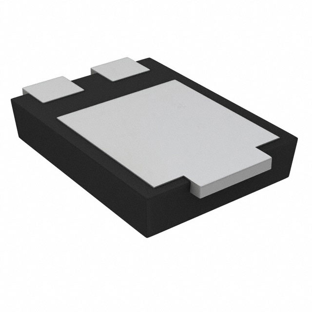
�FSV15100V
15 A, 100 V Ultra-Low VF Schottky Rectifier
Features
•
•
•
•
•
•
•
•
Ultra-Low Forward Voltage Drop
Low Thermal Resistance
Very Low Profile: Typical Height of 1.1 mm
Trench Schottky Technology
RoHS Compliant
Green Molding Compound as per IEC61249 Standard
Lead Free in Compliance with EU RoHS 2011/65/EU Directive
Qualified per AEC-Q101 Rev. C Standard
3
2
TO-277
1
Anode 1
3
Anode 2
Cathode
Ordering Information
Part Number
Top Mark
Package
Packing Method
FSV15100V
FSV15100V
TO-277 3L
Tape and Reel
Absolute Maximum Ratings
Stresses exceeding the absolute maximum ratings may damage the device. The device may not function or be operable above the recommended operating conditions and stressing the parts to these levels is not recommended. In addition, extended exposure to stresses above the recommended operating conditions may affect device reliability. The
absolute maximum ratings are stress ratings only. Values are at TA = 25°C unless otherwise noted.
Symbol
Value
Unit
VRRM
Peak Repetitive Reverse Voltage
100
V
VRWM
Working Peak Reverse Voltage
100
V
VRMS
RMS Reverse Voltage
70
V
DC Blocking Voltage
100
V
Average Rectified Peak Forward Surge Current
15
A
VR
IF(AV)
IFSM
TJ
TSTG
Parameter
Non-Repetitive Peak Forward Surge Current
250
A
Operating Junction Temperature Range
-55 to +150
°C
Storage Temperature Range
-55 to +150
°C
© 2015 Fairchild Semiconductor Corporation
FSV15100V Rev. 1.1
www.fairchildsemi.com
FSV15100V — 15 A, 100 V Ultra-Low VF Schottky Rectifier
July 2015
�Values are at TA = 25°C unless otherwise noted.
Symbol
RθJA
ψJL
Minimum
Maximum
Land Pattern Land Pattern
Parameter
Junction-to-Ambient Thermal Resistance
100
40
Junction-to-Lead Thermal Characteristics,
Thermocouple Soldered to Anode
15
12
Junction-to-Lead Thermal Characteristics,
Thermocouple Soldered to Cathode
6
Unit
°C/W
°C/W
5
Note:
1. The thermal resistances (RθJA & ψJL) are characterized with device mounted on the following FR4 printed circuit
boards, as shown in Figure 1 and Figure 2. PCB size: 76.2 x 114.3 mm. Minimum land pattern size: 4.9 x 4.8 mm
(big pattern, x1), 1.4 x 1.52 mm (small pattern, x2). Maximum land pattern size: 30 x 30 mm (pattern, x2).
Force line trace size = 55 mils, sense line trace size = 4 mils.
F
S
F
S
F
S
F
S
F
S
Figure 1. Minimum Land Pattern of 2 oz Copper
Figure 2. Maximum Land Pattern of 2 oz Copper
Electrical Characteristics
Values are at TA = 25°C unless otherwise noted.
Symbol
Parameter
Conditions
BVR
Breakdown Voltage
IR = 0.5 mA
VF
Forward Voltage Drop
IF = 15 A
IR
Reverse Current
VR = 100 V
© 2015 Fairchild Semiconductor Corporation
FSV15100V Rev. 1.1
Min.
Typ.
Max.
100
Unit
V
0.613
0.660
V
28
80
μA
www.fairchildsemi.com
2
FSV15100V — 15 A, 100 V Ultra-Low VF Schottky Rectifier
Thermal Characteristics(1)
�100
100
IR - LEAKAGE CURRENT (mA)
IF - FORWARD CURRENT (A)
o
o
TA = 150 C
10
o
TA = 125 C
1
o
TA = 100 C
o
TA = 75 C
0.1
o
TA = 25 C
0.01
0.0
0.2
0.4
TA = 150 C
10
o
TA = 100 C
1
o
TA = 125 C
o
TA = 75 C
0.1
0.01
o
TA = 25 C
0.6
1E-3
20
0.8
VF - FORWARD VOLTAGE (V)
Figure 3. Typical Forward Characteristics
40
50
60
70
80
90
100
Figure 4. Typical Reverse Characteristics
18
2200
2000
IF - FORWARD CURRENT (A)
CJ - JUNCTION CAPACITANCE (pF)
30
PERCENT OF RATED REVERSE VOLTAGE (%)
1800
1600
1400
1200
1000
800
600
400
15
12
9
6
3
200
0
1
10
100
0
50
75
100
125
150
TC - CASE TEMPERATURE ( C)
Figure 5. Typical Junction Capacitance
© 2015 Fairchild Semiconductor Corporation
FSV15100V Rev. 1.1
25
o
VR - REVERSE BIAS VOLTAGE (V)
Figure 6. Forward Current Derating Curve
www.fairchildsemi.com
3
FSV15100V — 15 A, 100 V Ultra-Low VF Schottky Rectifier
Typical Performance Characteristics
�A
6.65
6.35
6.15
5.67
B
4.63
D 4.25
0.63
0.43 (2X)
TOP VIEW
SEATING
PLANE
0.01
4.65 MIN
1.40
1.10 (2X)
1.45 MIN
4.15 MIN
0.40
0.23
1.97
1.15 MIN
1.00
2.75
LAND PATTERN RECOMMENDATION
1.20
1.00
FRONT VIEW
(0.35)
C
D
4.90
4.23
1.25
0.90
2.20
2.00
4.15 2.25
D 3.25 1.95
NOTES: UNLESS OTHERWISE SPECIFIED
A. PACKAGE REFERENCE: JEDEC TO-277
B. DIMENSIONS ARE EXCLUSIVE OF
BURRS, MOLD FLASH, AND TIE BAR
EXTRUSIONS.
C. ALL DIMENSIONS ARE IN MILLIMETERS.
D
DOES NOT COMPLY TO JEDEC
STANDARD VALUE.
E. DRAWING FILENAME: MKT-TO277A03rev5
0.913
3.680
(0.25)
BOTTOM VIEW
0.60
DAP OPTION
4.75 MAX
BOTTOM VIEW - DAP OPTION
�ON Semiconductor and
are trademarks of Semiconductor Components Industries, LLC dba ON Semiconductor or its subsidiaries in the United States and/or other countries.
ON Semiconductor owns the rights to a number of patents, trademarks, copyrights, trade secrets, and other intellectual property. A listing of ON Semiconductor’s product/patent
coverage may be accessed at www.onsemi.com/site/pdf/Patent−Marking.pdf. ON Semiconductor reserves the right to make changes without further notice to any products herein.
ON Semiconductor makes no warranty, representation or guarantee regarding the suitability of its products for any particular purpose, nor does ON Semiconductor assume any liability
arising out of the application or use of any product or circuit, and specifically disclaims any and all liability, including without limitation special, consequential or incidental damages.
Buyer is responsible for its products and applications using ON Semiconductor products, including compliance with all laws, regulations and safety requirements or standards,
regardless of any support or applications information provided by ON Semiconductor. “Typical” parameters which may be provided in ON Semiconductor data sheets and/or
specifications can and do vary in different applications and actual performance may vary over time. All operating parameters, including “Typicals” must be validated for each customer
application by customer’s technical experts. ON Semiconductor does not convey any license under its patent rights nor the rights of others. ON Semiconductor products are not
designed, intended, or authorized for use as a critical component in life support systems or any FDA Class 3 medical devices or medical devices with a same or similar classification
in a foreign jurisdiction or any devices intended for implantation in the human body. Should Buyer purchase or use ON Semiconductor products for any such unintended or unauthorized
application, Buyer shall indemnify and hold ON Semiconductor and its officers, employees, subsidiaries, affiliates, and distributors harmless against all claims, costs, damages, and
expenses, and reasonable attorney fees arising out of, directly or indirectly, any claim of personal injury or death associated with such unintended or unauthorized use, even if such
claim alleges that ON Semiconductor was negligent regarding the design or manufacture of the part. ON Semiconductor is an Equal Opportunity/Affirmative Action Employer. This
literature is subject to all applicable copyright laws and is not for resale in any manner.
PUBLICATION ORDERING INFORMATION
LITERATURE FULFILLMENT:
Literature Distribution Center for ON Semiconductor
19521 E. 32nd Pkwy, Aurora, Colorado 80011 USA
Phone: 303−675−2175 or 800−344−3860 Toll Free USA/Canada
Fax: 303−675−2176 or 800−344−3867 Toll Free USA/Canada
Email: orderlit@onsemi.com
© Semiconductor Components Industries, LLC
N. American Technical Support: 800−282−9855 Toll Free
USA/Canada
Europe, Middle East and Africa Technical Support:
Phone: 421 33 790 2910
Japan Customer Focus Center
Phone: 81−3−5817−1050
www.onsemi.com
1
ON Semiconductor Website: www.onsemi.com
Order Literature: http://www.onsemi.com/orderlit
For additional information, please contact your local
Sales Representative
www.onsemi.com
�