HUF76439S3S
October 2013
Data Sheet
N-Channel Logic Level UltraFET Power MOSFET
60 V, 71 A, 14 mΩ
Packaging
Features
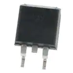
JEDEC TO-263AB
DRAIN
(FLANGE)
GATE
SOURCE
• Ultra Low On-Resistance
- rDS(ON) = 0.012Ω, VGS = 10V
- rDS(ON) = 0.014Ω, VGS = 5V
• Simulation Models
- Temperature Compensated PSPICE® and SABER™
Electrical Models
- Spice and SABER Thermal Impedance Models
- www.fairchildsemi.com
• Peak Current vs Pulse Width Curve
• UIS Rating Curve
Symbol
• Switching Time vs RGS Curves
D
Ordering Information
PART NUMBER
HUF76439S3ST
G
PACKAGE
TO-263AB
BRAND
76439S
S
Absolute Maximum Ratings
TC = 25oC, Unless Otherwise Specified
HUF76439S3ST
UNITS
Drain to Source Voltage (Note 1). . . . . . . . . . . . . . . . . . . . . . . . . . . . . . . . . . . . . . . . . . VDSS
60
V
Drain to Gate Voltage (RGS = 20kΩ) (Note 1) . . . . . . . . . . . . . . . . . . . . . . . . . . . . . . . VDGR
Gate to Source Voltage . . . . . . . . . . . . . . . . . . . . . . . . . . . . . . . . . . . . . . . . . . . . . . . . . . VGS
60
V
±16
V
Drain Current
Continuous (TC = 25oC, VGS = 5V) . . . . . . . . . . . . . . . . . . . . . . . . . . . . . . . . . . . . . . . . ID
Continuous (TC = 25oC, VGS = 10V) (Figure 2) . . . . . . . . . . . . . . . . . . . . . . . . . . . . . . . ID
Continuous (TC = 100oC, VGS = 5V) . . . . . . . . . . . . . . . . . . . . . . . . . . . . . . . . . . . . . . . ID
Continuous (TC = 100oC, VGS = 4.5V) (Figure 2) . . . . . . . . . . . . . . . . . . . . . . . . . . . . . . ID
Pulsed Drain Current . . . . . . . . . . . . . . . . . . . . . . . . . . . . . . . . . . . . . . . . . . . . . . . . . . IDM
75
75
54
52
Figure 4
A
A
A
A
Pulsed Avalanche Rating . . . . . . . . . . . . . . . . . . . . . . . . . . . . . . . . . . . . . . . . . . . . . . . . UIS
Figures 6, 17, 18
Power Dissipation . . . . . . . . . . . . . . . . . . . . . . . . . . . . . . . . . . . . . . . . . . . . . . . . . . . . . . . PD
Derate Above 25oC . . . . . . . . . . . . . . . . . . . . . . . . . . . . . . . . . . . . . . . . . . . . . . . . . . . . . .
180
1.20
W
W/oC
Operating and Storage Temperature. . . . . . . . . . . . . . . . . . . . . . . . . . . . . . . . . . . . TJ, TSTG
-55 to 175
oC
Maximum Temperature for Soldering
Leads at 0.063in (1.6mm) from Case for 10s. . . . . . . . . . . . . . . . . . . . . . . . . . . . . . . . . T L
Package Body for 10s, See Techbrief TB334. . . . . . . . . . . . . . . . . . . . . . . . . . . . . . . T pkg
300
260
oC
oC
NOTES:
1. TJ = 25oC to 150oC.
CAUTION: Stresses above those listed in “Absolute Maximum Ratings” may cause permanent damage to the device. This is a stress only rating and operation of the
device at these or any other conditions above those indicated in the operational sections of this specification is not implied.
Product reliability information can be found at http://www.fairchildsemi.com/products/discrete/reliability/index.html
For severe environments, see our Automotive HUFA series.
All Fairchild semiconductor products are manufactured, assembled and tested under ISO9000 and QS9000 quality systems certification.
©2001 Fairchild Semiconductor Corporation
HUF76439S3S Rev. C0
�HUF76439S3S
Electrical Specifications
TC = 25oC, Unless Otherwise Specified
PARAMETER
SYMBOL
TEST CONDITIONS
MIN
TYP
MAX
UNITS
ID = 250µA, VGS = 0V (Figure 12)
60
-
-
V
ID = 250µA, VGS = 0V , T C = -40oC (Figure 12)
55
-
-
V
VDS = 55V, VGS = 0V
-
-
1
µA
VDS = 50V, VGS = 0V, TC = 150oC
-
-
250
µA
VGS = ±16V
-
-
±100
nA
OFF STATE SPECIFICATIONS
Drain to Source Breakdown Voltage
Zero Gate Voltage Drain Current
Gate to Source Leakage Current
BVDSS
IDSS
IGSS
ON STATE SPECIFICATIONS
Gate to Source Threshold Voltage
VGS(TH)
VGS = VDS, ID = 250µA (Figure 11)
1
-
3
V
Drain to Source On Resistance
rDS(ON)
ID = 75A, VGS = 10V (Figures 9, 10)
-
0.010
0.012
Ω
ID = 54A, VGS = 5V (Figure 9)
-
0.0117
0.014
Ω
ID = 52A, VGS = 4.5V (Figure 9)
-
0.0125
0.015
Ω
TO-263AB
-
-
0.96
oC/W
-
-
62
oC/W
THERMAL SPECIFICATIONS
Thermal Resistance Junction to Case
RθJC
Thermal Resistance Junction to
Ambient
RθJA
SWITCHING SPECIFICATIONS (VGS = 4.5V)
Turn-On Time
Turn-On Delay Time
tON
td(ON)
-
470
ns
16
-
ns
tr
-
300
-
ns
-
29
-
ns
tf
-
105
-
ns
tOFF
-
-
200
ns
-
-
205
ns
Fall Time
Turn-Off Time
-
td(OFF)
Rise Time
Turn-Off Delay Time
VDD = 30V, ID = 52A
VGS = 4.5V, RGS = 3.9Ω
(Figures 15, 21, 22)
SWITCHING SPECIFICATIONS (VGS = 10V)
Turn-On Time
Turn-On Delay Time
Rise Time
tON
td(ON)
tr
Turn-Off Delay Time
Fall Time
Turn-Off Time
VDD = 30V, ID = 75A
VGS = 10V,
RGS = 3.9Ω
(Figures 16, 21, 22)
-
11
-
ns
-
125
-
ns
td(OFF)
-
45
-
ns
tf
-
125
-
ns
tOFF
-
-
255
ns
GATE CHARGE SPECIFICATIONS
Total Gate Charge
Qg(TOT)
VGS = 0V to 10V
Gate Charge at 5V
Qg(5)
VGS = 0V to 5V
Qg(TH)
VGS = 0V to 1V
VDD = 30V,
ID = 50A,
Ig(REF) = 1.0mA
-
70
84
nC
-
38
45
nC
-
2.5
3
nC
Gate to Source Gate Charge
Qgs
-
8
-
nC
Gate to Drain “Miller” Charge
Qgd
-
19
-
nC
Threshold Gate Charge
(Figures 14, 19, 20)
CAPACITANCE SPECIFICATIONS
Input Capacitance
CISS
Output Capacitance
COSS
Reverse Transfer Capacitance
CRSS
VDS = 25V, VGS = 0V,
f = 1MHz
(Figure 13)
-
2745
-
pF
-
840
-
pF
-
145
-
pF
MIN
TYP
MAX
UNITS
ISD = 54A
-
-
1.25
V
ISD = 27A
-
-
1.00
V
Source to Drain Diode Specifications
PARAMETER
Source to Drain Diode Voltage
Reverse Recovery Time
Reverse Recovered Charge
©2001 Fairchild Semiconductor Corporation
SYMBOL
VSD
TEST CONDITIONS
trr
ISD = 54A, dISD/dt = 100A/µs
-
-
72
ns
QRR
ISD = 54A, dISD/dt = 100A/µs
-
-
140
nC
HUF76439S3S Rev. C0
�HUF76439S3S
Typical Performance Curves
80
1.0
ID, DRAIN CURRENT (A)
POWER DISSIPATION MULTIPLIER
1.2
0.8
0.6
0.4
VGS = 10V
60
VGS = 4.5V
40
20
0.2
0
0
25
50
75
100
150
125
0
175
25
50
75
TC , CASE TEMPERATURE (oC)
100
125
150
175
TC, CASE TEMPERATURE (oC)
FIGURE 1. NORMALIZED POWER DISSIPATION vs CASE
TEMPERATURE
FIGURE 2. MAXIMUM CONTINUOUS DRAIN CURRENT vs
CASE TEMPERATURE
2
ZθJC, NORMALIZED
THERMAL IMPEDANCE
1
DUTY CYCLE - DESCENDING ORDER
0.5
0.2
0.1
0.05
0.02
0.01
PDM
0.1
t1
t2
NOTES:
DUTY FACTOR: D = t1/t2
PEAK TJ = PDM x ZθJC x RθJC + TC
SINGLE PULSE
0.01
10-5
10-4
10-3
10-2
10-1
100
101
t, RECTANGULAR PULSE DURATION (s)
FIGURE 3. NORMALIZED MAXIMUM TRANSIENT THERMAL IMPEDANCE
IDM, PEAK CURRENT (A)
1000
TC = 25oC
FOR TEMPERATURES
ABOVE 25oC DERATE PEAK
CURRENT AS FOLLOWS:
175 - TC
I = I25
150
VGS = 10V
VGS = 5V
100
50
TRANSCONDUCTANCE
MAY LIMIT CURRENT
IN THIS REGION
10-5
10-4
10-3
10-2
10-1
100
101
t, PULSE WIDTH (s)
FIGURE 4. PEAK CURRENT CAPABILITY
©2001 Fairchild Semiconductor Corporation
HUF76439S3S Rev. C0
�HUF76439S3S
Typical Performance Curves
(Continued)
500
100
100µs
If R = 0
tAV = (L)(IAS)/(1.3*RATED BVDSS - VDD)
If R ≠ 0
tAV = (L/R)ln[(IAS*R)/(1.3*RATED BVDSS - VDD) +1]
IAS, AVALANCHE CURRENT (A)
ID, DRAIN CURRENT (A)
1000
100
OPERATION IN THIS
AREA MAY BE
LIMITED BY rDS(ON)
10
1ms
SINGLE PULSE
TJ = MAX RATED
TC = 25oC
1
1
10ms
10
STARTING TJ = 25oC
STARTING TJ = 150oC
10
0.01
100
0.1
1
10
tAV, TIME IN AVALANCHE (ms)
VDS, DRAIN TO SOURCE VOLTAGE (V)
NOTE: Refer to Fairchild Application Notes AN9321 and AN9322.
FIGURE 6. UNCLAMPED INDUCTIVE SWITCHING
CAPABILITY
FIGURE 5. FORWARD BIAS SAFE OPERATING AREA
150
PULSE DURATION = 80µs
DUTY CYCLE = 0.5% MAX
VDD = 15V
120
VGS = 10V
VGS = 5V
ID, DRAIN CURRENT (A)
ID, DRAIN CURRENT (A)
150
90
60
TJ = 175oC
30
TJ = -55oC
120
2.0
2.5
PULSE DURATION = 80µs
DUTY CYCLE = 0.5% MAX
TC = 25oC
90
60
VGS = 3.5V
30
VGS = 3V
TJ = 25oC
0
VGS = 4V
0
3.5
4.0
3.0
4.5
VGS, GATE TO SOURCE VOLTAGE (V)
0
5.0
FIGURE 7. TRANSFER CHARACTERISTICS
4
FIGURE 8. SATURATION CHARACTERISTICS
25
2.5
20
PULSE DURATION = 80µs
DUTY CYCLE = 0.5% MAX
TC = 25oC
NORMALIZED DRAIN TO SOURCE
ON RESISTANCE
ID = 75A
rDS(ON), DRAIN TO SOURCE
ON RESISTANCE (mΩ)
1
2
3
VDS, DRAIN TO SOURCE VOLTAGE (V)
ID = 50A
15
ID = 25A
10
5
PULSE DURATION = 80µs
DUTY CYCLE = 0.5% MAX
VGS = 10V, ID = 75A
2.0
1.5
1.0
0.5
2
4
6
8
VGS, GATE TO SOURCE VOLTAGE (V)
10
FIGURE 9. DRAIN TO SOURCE ON RESISTANCE vs GATE
VOLTAGE AND DRAIN CURRENT
©2001 Fairchild Semiconductor Corporation
-80
-40
160
0
40
80
120
TJ, JUNCTION TEMPERATURE (oC)
200
FIGURE 10. NORMALIZED DRAIN TO SOURCE ON
RESISTANCE vs JUNCTION TEMPERATURE
HUF76439S3S Rev. C0
�HUF76439S3S
Typical Performance Curves
(Continued)
1.2
1.2
ID = 250µA
NORMALIZED DRAIN TO SOURCE
BREAKDOWN VOLTAGE
NORMALIZED GATE
THRESHOLD VOLTAGE
VGS = VDS, ID = 250µA
1.0
0.8
0.6
1.1
1.0
0.4
0.9
-80
-40
0
40
80
120
160
200
-80
-40
TJ, JUNCTION TEMPERATURE (oC)
FIGURE 11. NORMALIZED GATE THRESHOLD VOLTAGE vs
JUNCTION TEMPERATURE
VGS , GATE TO SOURCE VOLTAGE (V)
C, CAPACITANCE (pF)
40
80
120
200
160
FIGURE 12. NORMALIZED DRAIN TO SOURCE BREAKDOWN
VOLTAGE vs JUNCTION TEMPERATURE
10
5000
CISS = CGS + CGD
CRSS = CGD
1000
0
TJ , JUNCTION TEMPERATURE (oC)
COSS ≅ CDS + CGD
100
VGS = 0V, f = 1MHz
VDD = 30V
8
6
4
WAVEFORMS IN
DESCENDING ORDER:
ID = 50A
ID = 25A
2
0
50
0.1
1.0
10
0
60
15
30
45
60
75
Qg, GATE CHARGE (nC)
VDS , DRAIN TO SOURCE VOLTAGE (V)
NOTE: Refer to Fairchild Application Notes AN7254 and AN7260.
FIGURE 13. CAPACITANCE vs DRAIN TO SOURCE VOLTAGE
FIGURE 14. GATE CHARGE WAVEFORMS FOR CONSTANT
GATE CURRENT
500
1000
VGS = 10V, VDD = 30V, ID = 75A
800
SWITCHING TIME (ns)
SWITCHING TIME (ns)
VGS = 4.5V, VDD = 30V, ID = 48A
tr
600
400
tf
200
10
20
30
40
RGS, GATE TO SOURCE RESISTANCE (Ω)
FIGURE 15. SWITCHING TIME vs GATE RESISTANCE
©2001 Fairchild Semiconductor Corporation
tf
300
tr
200
td(ON)
td(ON)
0
td(OFF)
100
td(OFF)
0
400
0
50
0
10
20
30
40
RGS, GATE TO SOURCE RESISTANCE (Ω)
50
FIGURE 16. SWITCHING TIME vs GATE RESISTANCE
HUF76439S3S Rev. C0
�HUF76439S3S
Test Circuits and Waveforms
VDS
BVDSS
L
tP
VARY tP TO OBTAIN
REQUIRED PEAK IAS
+
RG
VDS
IAS
VDD
VDD
-
VGS
DUT
tP
0V
IAS
0
0.01Ω
tAV
FIGURE 17. UNCLAMPED ENERGY TEST CIRCUIT
FIGURE 18. UNCLAMPED ENERGY WAVEFORMS
VDS
VDD
RL
Qg(TOT)
VDS
VGS = 10V
VGS
Qg(5)
+
VDD
VGS = 5V
VGS
DUT
VGS = 1V
Ig(REF)
0
Qg(TH)
Qgs
Qgd
Ig(REF)
0
FIGURE 19. GATE CHARGE TEST CIRCUIT
FIGURE 20. GATE CHARGE WAVEFORMS
VDS
tON
tOFF
td(ON)
td(OFF)
tr
RL
VDS
tf
90%
90%
+
VGS
VDD
-
10%
10%
0
DUT
90%
RGS
VGS
VGS
0
FIGURE 21. SWITCHING TIME TEST CIRCUIT
©2001 Fairchild Semiconductor Corporation
10%
50%
50%
PULSE WIDTH
FIGURE 22. SWITCHING TIME WAVEFORM
HUF76439S3S Rev. C0
�HUF76439S3S
PSPICE Electrical Model
.SUBCKT HUF76439 2 1 3 ;
rev 17 June 1999
CA 12 8 3.70e-9
CB 15 14 3.80e-9
CIN 6 8 2.60e-9
LDRAIN
DBODY 7 5 DBODYMOD
DBREAK 5 11 DBREAKMOD
DPLCAP 10 5 DPLCAPMOD
DPLCAP
10
RLDRAIN
RSLC1
51
DBREAK
+
EBREAK 11 7 17 18 66.25
EDS 14 8 5 8 1
EGS 13 8 6 8 1
ESG 6 10 6 8 1
EVTHRES 6 21 19 8 1
EVTEMP 20 6 18 22 1
RSLC2
5
51
ESLC
11
-
RDRAIN
6
8
ESG
EVTHRES
+ 19 8
+
LGATE
GATE
1
+
50
-
IT 8 17 1
LDRAIN 2 5 1.0e-9
LGATE 1 9 5.17e-9
LSOURCE 3 7 2.33e-9
DRAIN
2
5
EVTEMP
RGATE +
18 22
9
20
21
EBREAK
17
18
DBODY
-
16
MWEAK
6
MMED
MSTRO
RLGATE
MMED 16 6 8 8 MMEDMOD
MSTRO 16 6 8 8 MSTROMOD
MWEAK 16 21 8 8 MWEAKMOD
LSOURCE
CIN
8
SOURCE
3
7
RSOURCE
RLSOURCE
RBREAK 17 18 RBREAKMOD 1
RDRAIN 50 16 RDRAINMOD 4.72e-3
RGATE 9 20 0.88
RLDRAIN 2 5 10
RLGATE 1 9 51.7
RLSOURCE 3 7 23.3
RSLC1 5 51 RSLCMOD 1e-6
RSLC2 5 50 1e3
RSOURCE 8 7 RSOURCEMOD 4.43e-3
RVTHRES 22 8 RVTHRESMOD 1
RVTEMP 18 19 RVTEMPMOD 1
S1A
12
S2A
14
13
13
8
S1B
CA
RBREAK
15
17
18
RVTEMP
S2B
13
CB
6
8
EGS
19
-
-
IT
14
+
+
VBAT
5
8
EDS
-
+
8
22
S1A
S1B
S2A
S2B
6 12 13 8 S1AMOD
13 12 13 8 S1BMOD
6 15 14 13 S2AMOD
13 15 14 13 S2BMOD
RVTHRES
VBAT 22 19 DC 1
ESLC 51 50 VALUE={(V(5,51)/ABS(V(5,51)))*(PWR(V(5,51)/(1e-6*225),3.5))}
.MODEL DBODYMOD D (IS = 2.52e-12 RS = 3.53e-3 TRS1 = 1.79e-3 TRS2 = 1.27e-6 CJO = 2.82e-9 TT = 4.90e-8 M = 0.43)
.MODEL DBREAKMOD D (RS = 1.95e- 1TRS1 = 9.01e- 4TRS2 = 2.07e-6)
.MODEL DPLCAPMOD D (CJO = 2.28e- 9IS = 1e-30 M = 0.85)
.MODEL MMEDMOD NMOS (VTO = 1.88 KP = 2.1 IS = 1e-30 N = 10 TOX = 1 L = 1u W = 1u RG = 0.88)
.MODEL MSTROMOD NMOS (VTO = 2.31 KP = 137 IS = 1e-30 N = 10 TOX = 1 L = 1u W = 1u)
.MODEL MWEAKMOD NMOS (VTO = 1.65 KP = 0.05 IS = 1e-30 N = 10 TOX = 1 L = 1u W = 1u RG = 8.8 RS = 0.1)
.MODEL RBREAKMOD RES (TC1 = 1.19e- 3TC2 = -1.91e-7)
.MODEL RDRAINMOD RES (TC1 = 1.15e-2 TC2 = 3.07e-5)
.MODEL RSLCMOD RES (TC1 = 9.92e-4 TC2 = 1.23e-6)
.MODEL RSOURCEMOD RES (TC1 = 0 TC2 = 0)
.MODEL RVTHRESMOD RES (TC1 = -2.65e-3 TC2 = -7.94e-6)
.MODEL RVTEMPMOD RES (TC1 = -1.39e- 3TC2 = -2.13e-7)
.MODEL S1AMOD VSWITCH (RON = 1e-5
.MODEL S1BMOD VSWITCH (RON = 1e-5
.MODEL S2AMOD VSWITCH (RON = 1e-5
.MODEL S2BMOD VSWITCH (RON = 1e-5
ROFF = 0.1
ROFF = 0.1
ROFF = 0.1
ROFF = 0.1
VON = -6.0 VOFF= -2.5)
VON = -2.5 VOFF= -6.0)
VON = -0.5 VOFF= 0.0)
VON = 0.0 VOFF= -0.5)
.ENDS
NOTE: For further discussion of the PSPICE model, consult A New PSPICE Sub-Circuit for the Power MOSFET Featuring Global
Temperature Options; IEEE Power Electronics Specialist Conference Records, 1991, written by William J. Hepp and C. Frank Wheatley.
©2001 Fairchild Semiconductor Corporation
HUF76439S3S Rev. C0
�HUF76439S3S
SABER Electrical Model
REV 17 June 1999
template ta76445 n2,n1,n3
electrical n2,n1,n3
{
var i iscl
d..model dbodymod = (is = 2.52e-12, cjo = 2.82e-9, tt = 4.90e-8, m = 0.43)
d..model dbreakmod = ()
d..model dplcapmod = (cjo = 2.28e-9, is = 1e-30, m = 0.85 )
m..model mmedmod = (type=_n, vto = 1.88, kp = 2.1, is = 1e-30, tox = 1)
m..model mstrongmod = (type=_n, vto = 2.31, kp = 137, is = 1e-30, tox = 1)
m..model mweakmod = (type=_n, vto = 1.65, kp = 0.05, is = 1e-30, tox = 1)
sw_vcsp..model s1amod = (ron = 1e-5, roff = 0.1, von = -6, voff = -2.5)
sw_vcsp..model s1bmod = (ron =1e-5, roff = 0.1, von = -2.5, voff = -6)
sw_vcsp..model s2amod = (ron = 1e-5, roff = 0.1, von = -0.5, voff = 0)
sw_vcsp..model s2bmod = (ron = 1e-5, roff = 0.1, von = 0, voff = -0.5)
LDRAIN
DPLCAP
10
RSLC1
51
c.ca n12 n8 = 3.70e-9
c.cb n15 n14 = 3.80e-9
c.cin n6 n8 = 2.60e-9
RLDRAIN
RDBREAK
RSLC2
72
ISCL
RDRAIN
6
8
ESG
EVTHRES
+ 19 8
+
i.it n8 n17 = 1
LGATE
GATE
1
EVTEMP
RGATE + 18 22
9
20
MWEAK
MSTRO
CIN
DBODY
EBREAK
+
17
18
MMED
m.mmed n16 n6 n8 n8 = model=mmedmod, l=1u, w=1u
m.mstrong n16 n6 n8 n8 = model=mstrongmod, l=1u, w=1u
m.mweak n16 n21 n8 n8 = model=mweakmod, l=1u, w=1u
71
11
16
6
RLGATE
res.rbreak n17 n18 = 1, tc1 = 1.19e-3, tc2 = -1.91e-7
res.rdbody n71 n5 = 3.53e-3, tc1 = 1.79e-3, tc2 = 1.27e-6
res.rdbreak n72 n5 = 1.95e-1, tc1 = 9.01e-4, tc2 = 2.07e-6
res.rdrain n50 n16 = 4.72e-3, tc1 = 1.15e-2, tc2 = 3.07e-5
res.rgate n9 n20 = 0.88
res.rldrain n2 n5 = 10
res.rlgate n1 n9 = 51.7
res.rlsource n3 n7 = 23.3
res.rslc1 n5 n51 = 1e-6, tc1 = 9.92e-4, tc2 = 1.23e-6
res.rslc2 n5 n50 = 1e3
res.rsource n8 n7 = 4.43e-3, tc1 = 0, tc2 = 0
res.rvtemp n18 n19 = 1, tc1 = -1.39e-3, tc2 = -2.13e-7
res.rvthres n22 n8 = 1, tc1 = -2.65e-3, tc2 = -7.94e-6
21
RDBODY
DBREAK
50
-
d.dbody n7 n71 = model=dbodymod
d.dbreak n72 n11 = model=dbreakmod
d.dplcap n10 n5 = model=dplcapmod
l.ldrain n2 n5 = 1e-9
l.lgate n1 n9 = 5.17e-9
l.lsource n3 n7 = 2.33e-9
DRAIN
2
5
-
8
LSOURCE
7
SOURCE
3
RSOURCE
RLSOURCE
S1A
12
S2A
14
13
13
8
S1B
CA
RBREAK
15
17
18
RVTEMP
S2B
13
+
6
8
EGS
19
CB
+
-
-
IT
14
VBAT
5
8
EDS
-
+
8
22
RVTHRES
spe.ebreak n11 n7 n17 n18 = 66.25
spe.eds n14 n8 n5 n8 = 1
spe.egs n13 n8 n6 n8 = 1
spe.esg n6 n10 n6 n8 = 1
spe.evtemp n20 n6 n18 n22 = 1
spe.evthres n6 n21 n19 n8 = 1
sw_vcsp.s1a n6 n12 n13 n8 = model=s1amod
sw_vcsp.s1b n13 n12 n13 n8 = model=s1bmod
sw_vcsp.s2a n6 n15 n14 n13 = model=s2amod
sw_vcsp.s2b n13 n15 n14 n13 = model=s2bmod
v.vbat n22 n19 = dc=1
equations {
i (n51->n50) +=iscl
iscl: v(n51,n50) = ((v(n5,n51)/(1e-9+abs(v(n5,n51))))*((abs(v(n5,n51)*1e6/225))** 3.5))
}
}
©2001 Fairchild Semiconductor Corporation
HUF76439S3S Rev. C0
�HUF76439S3S
SPICE Thermal Model
th
JUNCTION
REV 23 June 1999
HUF76439T
CTHERM1 th 6 3.00e-3
CTHERM2 6 5 1.90e-2
CTHERM3 5 4 6.95e-3
CTHERM4 4 3 7.00e-3
CTHERM5 3 2 2.95e-2
CTHERM6 2 tl 12.55
RTHERM1
RTHERM1 th 6 6.32e-3
RTHERM2 6 5 1.57e-2
RTHERM3 5 4 4.43e-2
RTHERM4 4 3 2.49e-1
RTHERM5 3 2 3.75e-1
RTHERM6 2 tl 4.98e-2
RTHERM2
CTHERM1
6
CTHERM2
5
RTHERM3
CTHERM3
SABER Thermal Model
SABER thermal model HUF76445T
template thermal_model th tl
thermal_c th, tl
{
ctherm.ctherm1 th 6 = 3.00e-3
ctherm.ctherm2 6 5 = 1.90e-2
ctherm.ctherm3 5 4 = 6.95e-3
ctherm.ctherm4 4 3 = 7.00e-3
ctherm.ctherm5 3 2 = 2.95e-2
ctherm.ctherm6 2 tl = 12.55
rtherm.rtherm1 th 6 = 6.32e-3
rtherm.rtherm2 6 5 = 1.57e-2
rtherm.rtherm3 5 4 = 4.43e-2
rtherm.rtherm4 4 3 = 2.49e-1
rtherm.rtherm5 3 2 = 3.75e-1
rtherm.rtherm6 2 tl = 4.98e-2
}
4
RTHERM4
CTHERM4
3
RTHERM5
CTHERM5
2
RTHERM6
CTHERM6
tl
©2001 Fairchild Semiconductor Corporation
CASE
HUF76439S3S Rev. C0
�HUF76439S3S
TRADEMARKS
The following includes registered and unregistered trademarks and service marks, owned by Fairchild Semiconductor and/or its global subsidiaries, and is not
intended to be an exhaustive list of all such trademarks.
Sync-Lock™
F-PFS™
AccuPower™
®
FRFET®
AX-CAP®*
®*
®
SM
BitSiC™
Global Power Resource
PowerTrench
GreenBridge™
PowerXS™
Build it Now™
TinyBoost®
Green FPS™
Programmable Active Droop™
CorePLUS™
TinyBuck®
®
Green FPS™ e-Series™
QFET
CorePOWER™
TinyCalc™
QS™
Gmax™
CROSSVOLT™
TinyLogic®
GTO™
Quiet Series™
CTL™
TINYOPTO™
IntelliMAX™
RapidConfigure™
Current Transfer Logic™
TinyPower™
ISOPLANAR™
DEUXPEED®
™
TinyPWM™
Dual Cool™
Marking Small Speakers Sound Louder
TinyWire™
EcoSPARK®
Saving our world, 1mW/W/kW at a time™
and Better™
TranSiC™
EfficentMax™
SignalWise™
MegaBuck™
TriFault Detect™
ESBC™
SmartMax™
MICROCOUPLER™
TRUECURRENT®*
SMART START™
MicroFET™
®
SerDes™
Solutions for Your Success™
MicroPak™
SPM®
MicroPak2™
Fairchild®
STEALTH™
MillerDrive™
Fairchild Semiconductor®
UHC®
SuperFET®
MotionMax™
FACT Quiet Series™
®
Ultra FRFET™
SuperSOT™-3
mWSaver
FACT®
UniFET™
SuperSOT™-6
OptoHiT™
FAST®
VCX™
SuperSOT™-8
OPTOLOGIC®
FastvCore™
VisualMax™
OPTOPLANAR®
SupreMOS®
FETBench™
VoltagePlus™
SyncFET™
FPS™
XS™
tm
*Trademarks of System General Corporation, used under license by Fairchild Semiconductor.
DISCLAIMER
FAIRCHILD SEMICONDUCTOR RESERVES THE RIGHT TO MAKE CHANGES WITHOUT FURTHER NOTICE TO ANY PRODUCTS HEREIN TO IMPROVE
RELIABILITY, FUNCTION, OR DESIGN. FAIRCHILD DOES NOT ASSUME ANY LIABILITY ARISING OUT OF THE APPLICATION OR USE OF ANY
PRODUCT OR CIRCUIT DESCRIBED HEREIN; NEITHER DOES IT CONVEY ANY LICENSE UNDER ITS PATENT RIGHTS, NOR THE RIGHTS OF OTHERS.
THESE SPECIFICATIONS DO NOT EXPAND THE TERMS OF FAIRCHILD’S WORLDWIDE TERMS AND CONDITIONS, SPECIFICALLY THE WARRANTY
THEREIN, WHICH COVERS THESE PRODUCTS.
LIFE SUPPORT POLICY
FAIRCHILD’S PRODUCTS ARE NOT AUTHORIZED FOR USE AS CRITICAL COMPONENTS IN LIFE SUPPORT DEVICES OR SYSTEMS WITHOUT THE
EXPRESS WRITTEN APPROVAL OF FAIRCHILD SEMICONDUCTOR CORPORATION.
As used here in:
1. Life support devices or systems are devices or systems which, (a) are
intended for surgical implant into the body or (b) support or sustain life,
and (c) whose failure to perform when properly used in accordance with
instructions for use provided in the labeling, can be reasonably
expected to result in a significant injury of the user.
2.
A critical component in any component of a life support, device, or
system whose failure to perform can be reasonably expected to cause
the failure of the life support device or system, or to affect its safety or
effectiveness.
ANTI-COUNTERFEITING POLICY
Fairchild Semiconductor Corporation’s Anti-Counterfeiting Policy. Fairchild’s Anti-Counterfeiting Policy is also stated on our external website,
www.Fairchildsemi.com, under Sales Support.
Counterfeiting of semiconductor parts is a growing problem in the industry. All manufactures of semiconductor products are experiencing counterfeiting of their
parts. Customers who inadvertently purchase counterfeit parts experience many problems such as loss of brand reputation, substandard performance, failed
application, and increased cost of production and manufacturing delays. Fairchild is taking strong measures to protect ourselves and our customers from the
proliferation of counterfeit parts. Fairchild strongly encourages customers to purchase Fairchild parts either directly from Fairchild or from Authorized Fairchild
Distributors who are listed by country on our web page cited above. Products customers buy either from Fairchild directly or from Authorized Fairchild
Distributors are genuine parts, have full traceability, meet Fairchild’s quality standards for handing and storage and provide access to Fairchild’s full range of
up-to-date technical and product information. Fairchild and our Authorized Distributors will stand behind all warranties and will appropriately address and
warranty issues that may arise. Fairchild will not provide any warranty coverage or other assistance for parts bought from Unauthorized Sources. Fairchild is
committed to combat this global problem and encourage our customers to do their part in stopping this practice by buying direct or from authorized distributors.
PRODUCT STATUS DEFINITIONS
Definition of Terms
Datasheet Identification
Product Status
Definition
Advance Information
Formative / In Design
Datasheet contains the design specifications for product development. Specifications
may change in any manner without notice.
Preliminary
First Production
Datasheet contains preliminary data; supplementary data will be published at a later
date. Fairchild Semiconductor reserves the right to make changes at any time without
notice to improve design.
No Identification Needed
Full Production
Datasheet contains final specifications. Fairchild Semiconductor reserves the right to
make changes at any time without notice to improve the design.
Obsolete
Not In Production
Datasheet contains specifications on a product that is discontinued by Fairchild
Semiconductor. The datasheet is for reference information only.
Rev. I66
©2001 Fairchild Semiconductor Corporation
HUF76439S3S Rev. C0
�Mouser Electronics
Authorized Distributor
Click to View Pricing, Inventory, Delivery & Lifecycle Information:
onsemi:
HUF76439S3S
�


 工商网监
湘ICP备2023018690号
工商网监
湘ICP备2023018690号
