J309 / J310 / MMBFJ309 / MMBFJ310
MMBFJ309
MMBFJ310
J309
J310
G
S
G
S
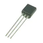
TO-92
SOT-23
D
D
Mark: 6U / 6T
NOTE: Source & Drain
are interchangeable
N-Channel RF Amplifier
This device is designed for VHF/UHF amplifier, oscillator and mixer
applications. As a common gate amplifier, 16 dB at 100 MHz and
12 dB at 450 MHz can be realized. Sourced from Process 92.
Absolute Maximum Ratings*
Symbol
TA = 25°C unless otherwise noted
Parameter
Value
Units
VDS
Drain-Source Voltage
25
V
VGS
Gate-Source Voltage
- 25
V
IGF
Forward Gate Current
10
mA
TJ ,Tstg
Operating and Storage Junction Temperature Range
-55 to +150
°C
*These ratings are limiting values above which the serviceability of any semiconductor device may be impaired.
NOTES:
1) These ratings are based on a maximum junction temperature of 150 degrees C.
2) These are steady state limits. The factory should be consulted on applications involving pulsed or low duty cycle operations.
Thermal Characteristics
Symbol
PD
TA = 25°C unless otherwise noted
Characteristic
RθJC
Total Device Dissipation
Derate above 25°C
Thermal Resistance, Junction to Case
RθJA
Thermal Resistance, Junction to Ambient
*Device mounted on FR-4 PCB 1.6" X 1.6" X 0.06."
1997 Fairchild Semiconductor Corporation
Max
Units
J309-J310
625
5.0
125
*MMBFJ309-310
350
2.8
357
556
mW
mW/°C
°C/W
°C/W
�(continued)
Electrical Characteristics
Symbol
TA = 25°C unless otherwise noted
Parameter
Test Conditions
Min
IG = - 1.0 µA, VDS = 0
VGS = - 15 V, VDS = 0
VGS = - 15 V, VDS = 0, TA =
125°C
VDS = 10 V, ID = 1.0 nA
- 25
Typ
Max Units
OFF CHARACTERISTICS
V(BR)GSS
Gate-Source Breakdown Voltage
IGSS
Gate Reverse Current
VGS(off)
Gate-Source Cutoff Voltage
V
- 1.0
- 1.0
nA
µA
309
310
- 1.0
- 2.0
- 4.0
- 6.5
V
V
309
310
12
24
30
60
1.0
mA
mA
V
ON CHARACTERISTICS
IDSS
VGS(f)
Zero-Gate Voltage Drain
Current*
Gate-Source Forward Voltage
VDS = 10 V, VGS = 0
VDS = 0, IG = 1.0 mA
J309 / J310 / MMBFJ309 / MMBFJ310
N-Channel RF Amplifier
SMALL SIGNAL CHARACTERISTICS
Re(yis)
Re(yos)
Gpg
Re(yfs)
Re(yig)
Common-Source Input
Conductance
Common-Source Output
Conductance
Common-Gate Power Gain
goss
0.7
0.5
0.25
VDS = 10, ID = 10 mA, f = 100 MHz
16
dB
12
mmhos
12
mmhos
Common-Source Output
Conductance
Common-Gate Forward
Conductance
VDS = 10, ID = 10 mA, f = 1.0 kHz
309
310
VDS = 10, ID = 10 mA, f = 1.0 kHz
20,000 µmhos
18,000 µmhos
150
µmhos
10,000
8000
Cdg
Drain-Gate Capacitance
VDS = 10, ID = 10 mA, f = 1.0 kHz
309
310
VDS = 10, ID = 10 mA, f = 1.0 kHz
309
310
VDS = 0, VGS = - 10 V, f = 1.0 MHz
Csg
NF
Source-Gate Capacitance
VDS = 0, VGS = - 10 V, f = 1.0 MHz
4.1
Noise Figure
3.0
en
Equivalent Short-Circuit Input
Noise Voltage
VDS = 10 V, ID = 10 mA,
f = 450 MHz
VDS = 10 V, ID = 10 mA,
f = 100 Hz
gfg
gog
mmhos
mmhos
mmhos
Common-Source Forward
VDS = 10, ID = 10 mA, f = 100 MHz
Transconductance
Common-Gate Input Conductance VDS = 10, ID = 10 mA, f = 100 MHz
Common-Source Forward
Transconductance
gfs
VDS = 10, ID = 10 mA, f = 100 MHz
309
310
VDS = 10, ID = 10 mA, f = 100 MHz
Common-Gate Output
Conductance
*Pulse Test: Pulse Width ≤ 300 µs, Duty Cycle ≤ 2.0%
13,000
12,000
µmhos
µmhos
100
150
2.0
2.5
µmhos
µmhos
pF
5.0
6.0
pF
dB
nV/√Hz
5
�(continued)
Typical Characteristics
Transfer Characteristics
Transfer Characteristics
Input Admittance
Transfer Characteristics
Transfer Characteristics
Forward Transadmittance
J309 / J310 / MMBFJ309 / MMBFJ310
N-Channel RF Amplifier
�(continued)
Typical Characteristics
(continued)
Common Drain-Source
Output Conductance vs.
Drain Current
Output Admittance
Capacitance vs. Voltage
J309 / J310 / MMBFJ309 / MMBFJ310
N-Channel RF Amplifier
5
Noise Voltage vs. Frequency
Reverse Transadmittance
�(continued)
Typical Characteristics
(continued)
Transconductance vs.
Drain Current
Parameter Interactions
Leakage Current vs. Voltage
P D - POWER DISSIPATION (mW)
Power Dissipation vs
Ambient Temperature
700
600
TO-92
500
SOT-23
400
300
200
100
0
0
25
50
75
100
TEMPERATURE ( o C)
125
150
J309 / J310 / MMBFJ309 / MMBFJ310
N-Channel RF Amplifier
�TRADEMARKS
The following are registered and unregistered trademarks Fairchild Semiconductor owns or is authorized to use and is
not intended to be an exhaustive list of all such trademarks.
ACEx™
Bottomless™
CoolFET™
CROSSVOLT™
DOME™
E2CMOSTM
EnSignaTM
FACT™
FACT Quiet Series™
FAST
FASTr™
GlobalOptoisolator™
GTO™
HiSeC™
ISOPLANAR™
MICROWIRE™
OPTOLOGIC™
OPTOPLANAR™
PACMAN™
POP™
PowerTrench
QFET™
QS™
QT Optoelectronics™
Quiet Series™
SILENT SWITCHER
SMART START™
SuperSOT™-3
SuperSOT™-6
SuperSOT™-8
SyncFET™
TinyLogic™
UHC™
VCX™
DISCLAIMER
FAIRCHILD SEMICONDUCTOR RESERVES THE RIGHT TO MAKE CHANGES WITHOUT FURTHER
NOTICE TO ANY PRODUCTS HEREIN TO IMPROVE RELIABILITY, FUNCTION OR DESIGN. FAIRCHILD
DOES NOT ASSUME ANY LIABILITY ARISING OUT OF THE APPLICATION OR USE OF ANY PRODUCT
OR CIRCUIT DESCRIBED HEREIN; NEITHER DOES IT CONVEY ANY LICENSE UNDER ITS PATENT
RIGHTS, NOR THE RIGHTS OF OTHERS.
LIFE SUPPORT POLICY
FAIRCHILD’S PRODUCTS ARE NOT AUTHORIZED FOR USE AS CRITICAL COMPONENTS IN LIFE SUPPORT
DEVICES OR SYSTEMS WITHOUT THE EXPRESS WRITTEN APPROVAL OF FAIRCHILD SEMICONDUCTOR CORPORATION.
As used herein:
1. Life support devices or systems are devices or
2. A critical component is any component of a life
support device or system whose failure to perform can
systems which, (a) are intended for surgical implant into
be reasonably expected to cause the failure of the life
the body, or (b) support or sustain life, or (c) whose
support device or system, or to affect its safety or
failure to perform when properly used in accordance
with instructions for use provided in the labeling, can be
effectiveness.
reasonably expected to result in significant injury to the
user.
PRODUCT STATUS DEFINITIONS
Definition of Terms
Datasheet Identification
Product Status
Definition
Advance Information
Formative or
In Design
This datasheet contains the design specifications for
product development. Specifications may change in
any manner without notice.
Preliminary
First Production
This datasheet contains preliminary data, and
supplementary data will be published at a later date.
Fairchild Semiconductor reserves the right to make
changes at any time without notice in order to improve
design.
No Identification Needed
Full Production
This datasheet contains final specifications. Fairchild
Semiconductor reserves the right to make changes at
any time without notice in order to improve design.
Obsolete
Not In Production
This datasheet contains specifications on a product
that has been discontinued by Fairchild semiconductor.
The datasheet is printed for reference information only.
Rev. G
�