www.fairchildsemi.com
KA3524
SMPS Controller
Features
Description
•
•
•
•
•
•
The KA3524 regulating pulse width modulator contains
all of the control circuit necessary to implement switching
regulators of either polarity, transformer coupled DC to
DC converters, transformerless polarity converters and voltage doublers, as well as other power control applications.
This device includes a 5V voltage regulator capable of supplying up to 50mA to external circuit , a control amplifier, an oscillator, a pulse width modulator, a phase
splitting flip-flop, dual alternating output switch transistors,
and current limiting and shut-down circuit. Both the regulator output transistor and each output switch are internally
current limiting and, to limit junction temperature, aninternal thermal shutdown circuit is employed.
Complete PWM power control circuit
Operation beyond 100KHz
2% frequency stability with temperature
Total quiescent current less than 10mA
Single ended or push-pull outputs
Current limit amplifier provides external component
protection
• On-chip protection against excessive junction temperature
and output current
• 5V, 50mA linear regulator output available to user
16-DIP
1
Internal Block Diagram
Rev. 5.0
©2000 Fairchild Semiconductor International
�KA3524
Absolute Maximum Ratings
Parameter
Symbol
Value
Unit
Supply Voltage
VCC
40
V
Reference Output Current
IREF
50
mA
Output Current (Each Output)
IO
100
mA
Oscillator Charging Current (pin 6 or 7)
ICHG(OSC)
5
mA
Lead Temperature (Soldering, 10 sec)
TLEAD
300
°C
PD
1000
mW
Operating Temperature
TPOR
0 ~ +70
°C
Storage Temperature
TSTG
-65 ~ + 150
°C
Power Dissipation (TA = 25°C)
Electrical Characteristics
(VIN=20V, f=20KHz, TA = 0 to +70°C, unless otherwise specified)
Parameter
Symbol
Conditions
Min.
Typ.
Max.
Unit
VREF
-
4.6
5.0
5.4
V
REFERENCE SECTION
Reference Output Voltage
Line Regulation
∆VREF
VCC = 8V to 40V
-
10
30
mV
Load Regulation
∆VREF
IREF = 0 mA to 20 mA
-
20
50
mV
Ripple Rejection
RR
f = 120Hz, TA = 25°C
-
66
-
dB
Short-Circuit Output Current
ISC
VREF = 0, TA = 25°C
-
100
-
mA
Temperature Stability
STT
-
0.3
1
%
Long Term Stability
ST
TA = 25°C
-
20
-
mV/KHr
CT = 0.001uF, RT = 2KΩ
-
350
-
KHz
-
OSCILLATOR SECTION
Maximum Frequency
f(MAX)
Initial Accuracy
ACCUR
RT and CT constant
-
5
-
%
Frequency Change with Voltage
∆f/∆VCC
VCC = 8V to 40V, TA = 25°C
-
-
1
%
Over operating temperature range
-
-
2
%
Frequency Change with
Temperature
∆f/∆T
Clock Amplitude (Pin 3)
V(CLK)
TA = 25°C
-
3.5
-
V
Clock Width (Pin 3)
tW(CLK)
CT = 0.01uF, TA = 25°C
-
0.5
-
µs
ERROR AMPLIFIER SECTION
VIO
VCM = 2.5V
-
2
10
mV
Input Bias Current
Input Offset Voltage
IBIAS
VCM = 2.5V
-
2
10
µA
Open Loop Voltage Gain
GVO
60
80
-
dB
Common-Mode Input Voltage
VCM
TA = 25°C
1.8
-
3.4
V
CMRR
TA = 25°C
-
70
-
dB
BWSS
GV = 0dB, TA= 25°C
-
3
-
MHz
0.5
-
3.8
V
Common-Mode Rejection Ratio
Small Signal Bandwidth
Output Voltage Swing
2
VO(ERR)
-
TA = 25°C
�KA3524
Electrical Characteristics
(VIN=20V, f=20KHz, TA=0°C to +70°C, unless otherwise specified)
Parameter
Symbol
Conditions
Min. Typ. Max. Unit
COMPARATOR SECTION
Maximum Duty Cycle
D(MAX)
% Each output on
Input Threshold (Pin 9)
VTH1
Zero duty cycle
Input Threshold (Pin 9)
VTH2
Maximum duty cycle
Input Bias Current
IBIAS
-
45
-
-
%
-
1
-
V
-
3.5
-
V
-
1
-
µA
180
200
220
mV
CURRENT LIMITING SECTION
Sense Voltage
VSENSE
V2 - V1≥50mV
V9 = 2V, TA = 25°C
Temperature Coefficient of Vsense ∆VSENSE/∆T
-
-
0.2
-
mV/°C
Common-Mode Voltage
VCM
-
0.7
-
1
V
Collector-Emitter Voltage
VCEO
-
40
-
-
V
Collector Leakage Current
ILKG
VCE = 40V
-
0.1
50
µA
OUTPUT SECTION (EACHOUTPUT)
VCE(SAT)
IC = 50mA
-
1
2
V
Emitter Output Voltage
Saturation Voltage
VE
VC = 20V
17
18
-
V
Rise Time (10 to 90)
tR
RC = 2KΩ, TA = 25°C
-
0.2
-
µs
Fall Time (90 to 10)
tF
RC = 2KΩ, TA = 25°C
-
0.1
-
µs
VCC =40V, PINS 1,4,7,8,11
and 14 are grounded, V2=2V
All other inputs and Outputs open
-
5
10
mA
Supply Current
ICC
3
�KA3524
Application Information
Voltage Reference
An internal series regulator provides a nominal 5 volt output which is used both to generate a reference voltage and is
the regulated source for all the internal timing and controlling circuitry. This regulator may be bypassed for operation
from a fixed 5 volt supply by connecting pins 15 and 16 together to the input voltage. In this configuration, the maximum
input voltage is 6.0 volts.
This reference regulator may be used as a 5 volt source for other circuitry. It will provide up to 50mA of current itself
and can easily be expanded to higher current with an external PNP as shown in Figure 2.
Expanded Reference Current Capability
Oscillator
The oscillator in the KA3524 uses an external resistor (RT) to establish a constant charging current into an external capacitor
(CT), While this uses more current than a series connected PC, it provides a linear ramp voltage on the capacitor which is also
used as a reference for the comparator. The charging current is equal to 3.6V/RT and should be kept within the range of
approximately 30uA to 2mA, i.e., 1.8K< RT
很抱歉,暂时无法提供与“KA3524”相匹配的价格&库存,您可以联系我们找货
免费人工找货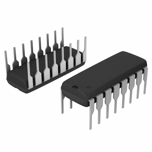


 工商网监
湘ICP备2023018690号
工商网监
湘ICP备2023018690号
