DATA SHEET
www.onsemi.com
Programmable Shunt
Regulator
3
KA431S, KA431SA,
KA431SL
1
2
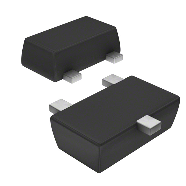
MF
1. Cathode
2. Ref
3. Anode
MF2
1. Ref
2. Cathode
3. Anode
SOT23−FL3L
CASE 318AB
DEVICE MARKING INFORMATION
Description
The KA431S / KA431SA / KA431SL are three−terminal adjustable
regulator series with a guaranteed thermal stability over the operating
temperature range. The output voltage can be set to any value between
VREF (approximately 2.5 V) and 36 V with two external resistors.
These devices have a typical dynamic output impedance of 0.2 W.
Active output circuitry provides a sharp turn−on characteristic,
making these devices excellent replacement for zener diodes in many
applications.
See general marking information in the device
marking section on page 2 of this data sheet.
ORDERING INFORMATION
See detailed ordering and shipping information on
page 6 of this data sheet.
Features
•
•
•
•
•
•
•
•
Programmable Output Voltage to 36 V
Low Dynamic Output Impedance 0.2 W (Typical)
Sink Current Capability: 1.0 to 100 mA
Equivalent Full−Range Temperature Coefficient of 50 ppm/°C
(Typical)
Temperature Compensated for Operation Over Full Rated Operating
Temperature Range
Low Output Noise Voltage
Fast Turn−on Response
These Devices are Pb−Free and Halogen Free
REFERENCE
CATHODE
+
−
2.5 Vref
ANODE
CATHODE (K)
REFERENCE (R)
ANODE(A)
Figure 1. Block Diagram
© Semiconductor Components Industries, LLC, 2002
May, 2022 − Rev. 8
1
Publication Order Number:
KA431SL/D
�KA431S, KA431SA, KA431SL
MARKING INFORMATION
MF −
43A
43B
43C
2% tolerance
1% tolerance
0.5% tolerance
43D
43E
43F
2% tolerance
1% tolerance
0.5% tolerance
MF2 −
Figure 2. Top Mark (per package)
ABSOLUTE MAXIMUM RATINGS
TA = 25°C unless otherwise noted
Parameter
Symbol
VKA
Cathode Voltage
Value
Unit
37
V
IKA
Cathode Current Range (Continuous)
−100 ~ +150
mA
IREF
Reference Input Current Range
−0.05 ~ +10
mA
RθJA
Thermal Resistance Junction−Air (Note 1) (Note 2)
MF Suffix Package
350
°C/W
IREF
Power Dissipation (Note 3) (Note 4)
MF Suffix Package
350
mW
150
_C
TOPR
TJ
Junction Temperature
Operating Temperature Range
−25 ~ +85
_C
TSTG
Storage Temperature Range
−65 ~ +150
_C
Stresses exceeding those listed in the Maximum Ratings table may damage the device. If any of these limits are exceeded, device functionality
should not be assumed, damage may occur and reliability may be affected.
1. Thermal resistance test board:
Size: 1.6 mm x 76.2 mm x 114.3 mm (1S0P))
JEDEC Standard: JESD51−3, JESD51−7
2. Assume no ambient airflow.
3. TJMAX = 150°C; Ratings apply to ambient temperature at 25°C.
4. Power dissipation calculation: PD = (TJ − TA) / RθJA.
RECOMMENDED OPERATING RANGES
Symbol
Parameter
Min.
Max.
Unit
VKA
Cathode Voltage
VREF
36
V
IKA
Cathode Current
1
100
mA
Functional operation above the stresses listed in the Recommended Operating Ranges is not implied. Extended exposure to stresses beyond
the Recommended Operating Ranges limits may affect device reliability.
www.onsemi.com
2
�KA431S, KA431SA, KA431SL
ELECTRICAL CHARACTERISTICS (Note 5)
Values are at TA = 25°C unless otherwise noted
KA431S
Min.
Symbol
Parameter
Conditions
VREF
Reference Input
Voltage
VKA = VREF, IKA = 10 mA
ΔVREF/ΔT
Deviation of Reference Input
Voltage Over−
Temperature
VKA = VREF, IKA = 10 mA,
TMIN ≤ TA ≤ TMAX
ΔVREF/ΔVKA
Ratio of Change
in Reference
Input Voltage
to the Change in
Cathode Voltage
IKA =
10 mA
Typ.
KA431SA
Max.
Min.
Typ.
KA431SL
Max.
Min.
Typ.
Max.
2.450 2.500 2.550 2.470 2.495 2.520 2.482 2.495 2.508
Unit
V
−
4.5
17.0
−
4.5
17.0
−
4.5
17.0
mV
ΔVKA =
10 V − VREF
−
−1.0
−2.7
−
−1.0
−2.7
−
−1.0
−2.7
mV/V
ΔVKA =
36 V − 10 V
−
−0.5
−2.0
−
−0.5
−2.0
−
−0.5
−2.0
IREF
Reference Input
Current
IKA = 10 mA,
R1 = 10 kW, R2 = ∞
−
1.5
4.0
−
1.5
4.0
−
1.5
4.0
mA
ΔIREF/ΔT
Deviation of
Reference Input
Current Over Full
Temperature
Range
IKA = 10 mA,
R1 = 10 kW, R2 = ∞
TA = Full Range
−
0.4
1.2
−
0.4
1.2
−
0.4
1.2
mA
IKA(MIN)
Minimum
Cathode Current
for Regulation
VKA = VREF
−
0.45
1.00
−
0.45
1.00
−
0.45
1.00
mA
IKA(OFF)
Off-Stage
Cathode Current
VKA = 36 V, VREF = 0
−
0.05
1.00
−
0.05
1.00
−
0.05
1.00
mA
VKA = VREF,
IKA = 1 to 100 mA,
f ≥ 1.0 kHz
−
0.15
0.50
−
0.15
0.50
−
0.15
0.50
W
ZKA
Dynamic
Impedance
Product parametric performance is indicated in the Electrical Characteristics for the listed test conditions, unless otherwise noted. Product
performance may not be indicated by the Electrical Characteristics if operated under different conditions.
5. TMIN = −25°C, TMAX = +85°C
TEST CIRCUITS
VKA
INPUT
VKA
INPUT
IKA
IKA
KA431S
VREF
R1
IREF
R2
VREF
KA431S
VKA = VREF (1 + R1/R2) + IREF R1
Figure 3. Test Circuit for VKA = VREF
INPUT
Figure 4. Test Circuit for VKA . VREF
VKA
IKA(OFF)
KA431S
Figure 5. Test Circuit for IKA(OFF)
www.onsemi.com
3
�KA431S, KA431SA, KA431SL
TYPICAL APPLICATIONS
ǒ
VO + 1 )
Ǔ
ǒ
R1
V ref
R2
VO + 1 )
VI
VO
VI
R1
VREF
Ǔ
R1
V ref
R2
IN
KA70805 OUT
COMMON
VO
R1
R2
KA431S
KA431S
Figure 6. Shunt Regulator
ǒ
VO + 1 )
R2
Figure 7. Output Control for Three−Terminal Fixed
Regulator
Ǔ
R1
V ref
R2
IO +
VI
VO
VI
V REF
R CL
RCL
IO
R1
KA431S
R2
KA431S
Figure 9. Current limit or Current Source
Figure 8. High Current Shunt Regulator
IO +
VI
V REF
RS
IO
KA431S
RS
Figure 10. Constant−Current Sink
www.onsemi.com
4
�KA431S, KA431SA, KA431SL
TYPICAL CHARACTERISTICS
800
VKA = VREF
TA = 25°C
100
IKA − Cathode Current (mA)
IK − Cathode Current (mA)
150
50
0
−50
−100
−2
−1
0
1
2
VKA = VREF
TA = 25°C
600
400
IKA(MIN)
200
0
−200
−1
3
0
VKA − Cathode Voltage (V)
0.20
3
3.5
0.18
0.16
0.14
0.12
0.10
0.08
0.06
0.04
0.02
0.00
−50
−25
0
25
50
75
100
125
150
3.0
2.5
2.0
1.5
1.0
0.5
0.0
−50
−25
0
TA − Ambient Temperature (5C)
25
50
75
100
125
TA − Ambient Temperature (5C)
Figure 13. OFF−State Cathode Current vs.
Ambient Temperature
Figure 14. Reference Input Current vs. Ambient
Temperature
6
60
TA = 25°C
TA = 25°C
IKA = 10 mA
50
5
40
Voltage Swing (V)
Open Loop Voltage Gain (dB)
2
Figure 12. Cathode Current vs. Cathode Voltage
Iref − Reference Input Current (mA)
Ioff − Off−State Cathode Current (mA)
Figure 11. Cathode Current vs. Cathode Voltage
30
20
10
INPUT
4
3
OUTPUT
2
1
0
−10
1
VKA − Cathode Voltage (V)
1k
10k
100k
1M
10M
0
0
Frequency (Hz)
4
8
12
Time (ms)
Figure 15. Frequency vs. Small Signal
Voltage Amplification
Figure 16. Pulse Response
www.onsemi.com
5
16
20
�KA431S, KA431SA, KA431SL
TYPICAL CHARACTERISTICS (Continued)
120
A
100
5
A: VKA = Vref
B: VKA = 5.0 V
@ IK = 10 mA
TA = 25°C
4
Current (mA)
IK − Cathode Current (mA)
140
80
60
40
0
10p
1n
2
1
B
20
3
1m
100n
10n
0
10m
0.0
0.2
0.4
CL − Load Capacitance
1.0
1.2
1.4
1.6
1.8 2.0
2.51
VREF, Reference Input Voltage (V)
5
4
Current (mA)
0.8
Figure 18. Anode−Reference Diode Curve
Figure 17. Stability Boundary Conditions
3
2
1
0
0.0
0.6
Anode−Reference Voltage (V)
0.2
0.4
0.6
0.8
1.0
1.2
1.4
1.6
1.8
2.0
2.50
2.49
2.48
2.47
2.46
−50
Reference−Cathode Voltage (V)
−25
0
25
50
75
100
125
TA , Ambient Temperature (5C)
Figure 20. Reference Input Voltage vs. Ambient
Temperature
Figure 19. Reference−Cathode Diode Curve
ORDERING INFORMATION
Part Number
KA431SMFTF
Output Voltage
Tolerance
Operating
Temperature Range
2%
−25 to +85°C
KA431SMF2TF
KA431SAMFTF
Package
Shipping†
43A
SOT23−FL3L
(Pb−Free)
3000 / Tape and Reel
43D
1%
43B
0.5%
43C
KA431SAMF2TF
KA431SLMFTF
Top Mark
43E
KA431SLMF2TF
43F
†For information on tape and reel specifications, including part orientation and tape sizes, please refer to our Tape and Reel Packaging
Specifications Brochure, BRD8011/D.
www.onsemi.com
6
�MECHANICAL CASE OUTLINE
PACKAGE DIMENSIONS
SOT23−3L
CASE 318AB
ISSUE A
DATE 14 DEC 2021
GENERIC
MARKING DIAGRAM*
XXXM
1
XXX = Specific Device Code
M = Date Code
DOCUMENT NUMBER:
DESCRIPTION:
98AON27911H
SOT23−3L
*This information is generic. Please refer to
device data sheet for actual part marking.
Pb−Free indicator, “G” or microdot “G”, may
or may not be present. Some products may
not follow the Generic Marking.
Electronic versions are uncontrolled except when accessed directly from the Document Repository.
Printed versions are uncontrolled except when stamped “CONTROLLED COPY” in red.
PAGE 1 OF 1
onsemi and
are trademarks of Semiconductor Components Industries, LLC dba onsemi or its subsidiaries in the United States and/or other countries. onsemi reserves
the right to make changes without further notice to any products herein. onsemi makes no warranty, representation or guarantee regarding the suitability of its products for any particular
purpose, nor does onsemi assume any liability arising out of the application or use of any product or circuit, and specifically disclaims any and all liability, including without limitation
special, consequential or incidental damages. onsemi does not convey any license under its patent rights nor the rights of others.
© Semiconductor Components Industries, LLC, 2018
www.onsemi.com
�onsemi,
, and other names, marks, and brands are registered and/or common law trademarks of Semiconductor Components Industries, LLC dba “onsemi” or its affiliates
and/or subsidiaries in the United States and/or other countries. onsemi owns the rights to a number of patents, trademarks, copyrights, trade secrets, and other intellectual property.
A listing of onsemi’s product/patent coverage may be accessed at www.onsemi.com/site/pdf/Patent−Marking.pdf. onsemi reserves the right to make changes at any time to any
products or information herein, without notice. The information herein is provided “as−is” and onsemi makes no warranty, representation or guarantee regarding the accuracy of the
information, product features, availability, functionality, or suitability of its products for any particular purpose, nor does onsemi assume any liability arising out of the application or use
of any product or circuit, and specifically disclaims any and all liability, including without limitation special, consequential or incidental damages. Buyer is responsible for its products
and applications using onsemi products, including compliance with all laws, regulations and safety requirements or standards, regardless of any support or applications information
provided by onsemi. “Typical” parameters which may be provided in onsemi data sheets and/or specifications can and do vary in different applications and actual performance may
vary over time. All operating parameters, including “Typicals” must be validated for each customer application by customer’s technical experts. onsemi does not convey any license
under any of its intellectual property rights nor the rights of others. onsemi products are not designed, intended, or authorized for use as a critical component in life support systems
or any FDA Class 3 medical devices or medical devices with a same or similar classification in a foreign jurisdiction or any devices intended for implantation in the human body. Should
Buyer purchase or use onsemi products for any such unintended or unauthorized application, Buyer shall indemnify and hold onsemi and its officers, employees, subsidiaries, affiliates,
and distributors harmless against all claims, costs, damages, and expenses, and reasonable attorney fees arising out of, directly or indirectly, any claim of personal injury or death
associated with such unintended or unauthorized use, even if such claim alleges that onsemi was negligent regarding the design or manufacture of the part. onsemi is an Equal
Opportunity/Affirmative Action Employer. This literature is subject to all applicable copyright laws and is not for resale in any manner.
PUBLICATION ORDERING INFORMATION
LITERATURE FULFILLMENT:
Email Requests to: orderlit@onsemi.com
onsemi Website: www.onsemi.com
◊
TECHNICAL SUPPORT
North American Technical Support:
Voice Mail: 1 800−282−9855 Toll Free USA/Canada
Phone: 011 421 33 790 2910
Europe, Middle East and Africa Technical Support:
Phone: 00421 33 790 2910
For additional information, please contact your local Sales Representative
�