Is Now Part of
To learn more about ON Semiconductor, please visit our website at
www.onsemi.com
Please note: As part of the Fairchild Semiconductor integration, some of the Fairchild orderable part numbers
will need to change in order to meet ON Semiconductor’s system requirements. Since the ON Semiconductor
product management systems do not have the ability to manage part nomenclature that utilizes an underscore
(_), the underscore (_) in the Fairchild part numbers will be changed to a dash (-). This document may contain
device numbers with an underscore (_). Please check the ON Semiconductor website to verify the updated
device numbers. The most current and up-to-date ordering information can be found at www.onsemi.com. Please
email any questions regarding the system integration to Fairchild_questions@onsemi.com.
ON Semiconductor and the ON Semiconductor logo are trademarks of Semiconductor Components Industries, LLC dba ON Semiconductor or its subsidiaries in the United States and/or other countries. ON Semiconductor owns the rights to a number
of patents, trademarks, copyrights, trade secrets, and other intellectual property. A listing of ON Semiconductor’s product/patent coverage may be accessed at www.onsemi.com/site/pdf/Patent-Marking.pdf. ON Semiconductor reserves the right
to make changes without further notice to any products herein. ON Semiconductor makes no warranty, representation or guarantee regarding the suitability of its products for any particular purpose, nor does ON Semiconductor assume any liability
arising out of the application or use of any product or circuit, and specifically disclaims any and all liability, including without limitation special, consequential or incidental damages. Buyer is responsible for its products and applications using ON
Semiconductor products, including compliance with all laws, regulations and safety requirements or standards, regardless of any support or applications information provided by ON Semiconductor. “Typical” parameters which may be provided in ON
Semiconductor data sheets and/or specifications can and do vary in different applications and actual performance may vary over time. All operating parameters, including “Typicals” must be validated for each customer application by customer’s
technical experts. ON Semiconductor does not convey any license under its patent rights nor the rights of others. ON Semiconductor products are not designed, intended, or authorized for use as a critical component in life support systems or any FDA
Class 3 medical devices or medical devices with a same or similar classification in a foreign jurisdiction or any devices intended for implantation in the human body. Should Buyer purchase or use ON Semiconductor products for any such unintended
or unauthorized application, Buyer shall indemnify and hold ON Semiconductor and its officers, employees, subsidiaries, affiliates, and distributors harmless against all claims, costs, damages, and expenses, and reasonable attorney fees arising out
of, directly or indirectly, any claim of personal injury or death associated with such unintended or unauthorized use, even if such claim alleges that ON Semiconductor was negligent regarding the design or manufacture of the part. ON Semiconductor
is an Equal Opportunity/Affirmative Action Employer. This literature is subject to all applicable copyright laws and is not for resale in any manner.
�www.fairchildsemi.com
KA7500B
SMPS Controller
Features
Description
• Internal Regulator Provides a Stable 5V Reference Supply
Trimmed to 5%
• Uncommitted Output TR for 200mA Sink or Source
Current
• Output Control For Push-Pull or Single Ended Operation
• Variable Duty Cycle By Dead Time Control (Pin 4)
Complete PWM Control Circuit
• On-Chip Oscillator With Master or Slave Operation
• Internal Circuit Prohibits Double Pulse at Either Output
The KA7500B is used for the control circuit of the PWM
switching regulator. The KA7500B consists of 5V reference
voltage circuit, two error amplifiers, a flip flop, an output
control circuit, a PWM comparator, a dead time comparator
and an oscillator. This device can be operated in the
switching frequency of 1kHz to 300kHz.
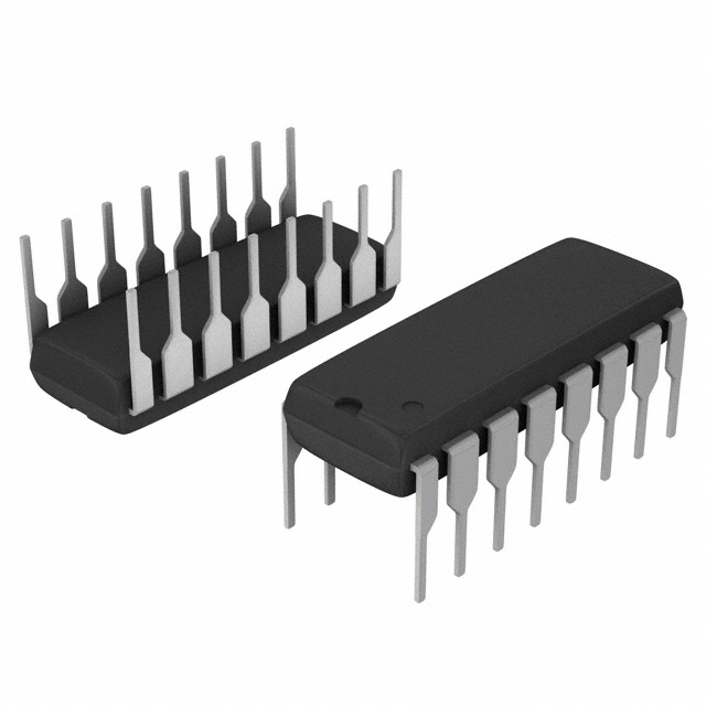
16-DIP
1
16-SOP
1
Internal Block Diagram
Rev. 1.0.0
©2002 Fairchild Semiconductor Corporation
�KA7500B
Absolute Maximum Ratings
Parameter
Value
Unit
VCC
42
V
Collector Supply Voltage
VC
42
V
Output Current
IO
250
mA
Amplifier Input Voltage
VIN
VCC +0.3
V
Power Dissipation (TA = 25°C)
PD
1 (KA7500B)
0.9 (KA7500BD)
W
Operating Temperature Range
TOPR
0 ~ +70
°C
Storage Temperature Range
TSTG
-65 ~ +150
°C
Supply Voltage
2
Symbol
�KA7500B
Electrical Characteristics
(VCC = 20V, f = 10kHz, TA = 0°C to +70°C, unless otherwise specified)
Parameter
Symbol
Conditions
Min.
Typ.
Max.
Unit
4.75
5.0
5.25
V
REFERENCE SECTION
Reference Output Voltage
VREF
∆VREF
VCC = 7V to 40V
-
2.0
25
mV
∆VREF/∆T
TA = 0°C to 70°C
-
0.01
0.03
%/°C
IREF = 1mA to 10mA
-
1.0
15
mV
10
35
50
mA
Line Regulation
Temperature Coefficient of VREF
IREF = 1mA
∆VREF
Load Regulation
Short-Circuit Output Current
ISC
VREF = 0V
OSCILLATOR SECTION
Oscillation Frequency
Frequency Change with Temperature
f
CT = 0.01µF, RT = 12kΩ
-
10
-
kHz
∆f/∆T
CT = 0.01µF, RT = 12kΩ
-
-
2
%
IBIAS
VCC = 15V, 0V≤V4≤5.25V
-
-2.0
-10
µA
45
-
-
%
Zero Duty Cycle
-
3.0
3.3
Max. Duty Cycle
0
-
-
DEAD TIME CONTROL SECTION
Input Bias Current
Maximum Duty Cycle
D(MAX)
Input Threshold Voltage
VITH
VCC = 15V, V4 = 0V
O.C Pin = VREF
V
ERROR AMP SECTION
Input Offset Voltage
VIO
V3 = 2.5V
-
2.0
10
mV
Input Offset Current
IIO
V3 = 2.5V
-
25
250
mA
Input Bias Current
IBIAS
V3 = 2.5V
-
0.2
1.0
µA
Common Mode Input Voltage
VCM
7V ≤ VCC ≤ 40V
-0.3
-
VCC
V
Open-Loop Voltage Gain
GVO
0.5V ≤ V3 ≤3 .5V
70
95
-
dB
Unit-Gain Bandwidth (Note1)
BW
-
-
650
-
kHz
Input Threshold Voltage
VITH
Zero Duty Cycle
Input Sink Current
ISINK
V3=0.7V
PWM COMPARATOR SECTION
-
4
4.5
V
-0.3
-0.7
-
mV
OUTPUT SECTION
Output Saturation Voltage
Common Emitter
VCE(SAT)
VE = 0, IC = 200mA
-
1.1
1.3
Common Collector
VCC(SAT)
VC = 15V, IE = -200mA
-
1.5
2.5
Collector Off-State Current
IC(OFF)
VCC = 40V, VCE = 40V
-
2
100
Emitter Off-State Current
IE(OFF)
VCC = VC = 40V, VE = 0
-
-
-100
ICC
Pin 6 = VREF, VCC = 15V
-
6
10
mA
-
V
µA
TOTAL DEVICE
Supply Current
OUTPUT SWITCHING CHARACTERISTICS
tR
-
-
-
-
Common Emitter
-
-
-
100
200
Common Collector
-
-
-
100
200
Fall Time
tF
-
-
-
-
Common Emitter
-
-
-
25
100
Common Collector
-
-
-
40
100
Rise Time
ns
ns
Note:
1. This parameter, although guaranteed, is not 100% tested in production.
3
�KA7500B
Typical Application
Pulse Width Modulated Step-down Converter
KSA1010
VI=10V to 40V
Vo=5V
Io=1A
1mH,2A
47Ω
150Ω
0.1uF
1MΩ
50uF
10V
5.1kΩ
12
Vcc
11
C2
8
C1
3
COMP INPUT
-2
VREF 14
5.1kΩ
- 15
KA7500B
5.1kΩ
+1
D.T GND E1
9
4
7
E2
10
O.C
13
RT
6
CT
5
+16
150Ω
+
+
50uF
50V
+
47kΩ
50uF
10V
0.001uF
GND
0.1
4
�KA7500B
Mechanical Dimensions
Package
16-DIP
#9
7.62
0.300
2.54
0.100
1.50 ±0.10
0.059 ±0.004
#8
0.46 ±0.10
0.018 ±0.004
#16
19.80
MAX
0.780
#1
19.40 ±0.20
0.764 ±0.008
(
0.81
)
0.032
6.40 ±0.20
0.252 ±0.008
3.25 ±0.20
0.128 ±0.008
5.08
MAX
0.200
0.38
0.014 MIN
3.30 ±0.30
0.130 ±0.012
+0.10
0~15°
0.25 –0.05
+0.004
0.010 –0.002
5
�KA7500B
Mechanical Dimensions (Continued)
Package
16-SOP
0.05
0.002
0.51
)
0.020
MIN
#9
0.70 ±0.20
0.0275 ±0.008
6
1.27
0.050
1.80
MAX
0.071
8°
MAX0.10
MAX0.004
3.95 ±0.20
0.156 ±0.008
0~
+0.10
0.20 -0.05
+0.004
0.008 -0.002
6.00 ±0.30
0.236 ±0.012
5.72
0.225
+0.10
0.406 -0.05
+0.004
0.016 -0.002
#8
9.90 ±0.20
0.39 ±0.008
#16
10.30
MAX
0.405
#1
(
1.55 ±0.10
0.061 ±0.004
�KA7500B
Ordering Information
Product Number
Package
KA7500B
16-DIP
KA7500BD
16-SOP
Operating Temperature
0 ~ +70°C
7
�KA7500B
DISCLAIMER
FAIRCHILD SEMICONDUCTOR RESERVES THE RIGHT TO MAKE CHANGES WITHOUT FURTHER NOTICE TO ANY
PRODUCTS HEREIN TO IMPROVE RELIABILITY, FUNCTION OR DESIGN. FAIRCHILD DOES NOT ASSUME ANY
LIABILITY ARISING OUT OF THE APPLICATION OR USE OF ANY PRODUCT OR CIRCUIT DESCRIBED HEREIN; NEITHER
DOES IT CONVEY ANY LICENSE UNDER ITS PATENT RIGHTS, NOR THE RIGHTS OF OTHERS.
LIFE SUPPORT POLICY
FAIRCHILD’S PRODUCTS ARE NOT AUTHORIZED FOR USE AS CRITICAL COMPONENTS IN LIFE SUPPORT DEVICES
OR SYSTEMS WITHOUT THE EXPRESS WRITTEN APPROVAL OF THE PRESIDENT OF FAIRCHILD SEMICONDUCTOR
CORPORATION. As used herein:
1. Life support devices or systems are devices or systems
which, (a) are intended for surgical implant into the body,
or (b) support or sustain life, and (c) whose failure to
perform when properly used in accordance with
instructions for use provided in the labeling, can be
reasonably expected to result in a significant injury of the
user.
2. A critical component in any component of a life support
device or system whose failure to perform can be
reasonably expected to cause the failure of the life support
device or system, or to affect its safety or effectiveness.
www.fairchildsemi.com
9/10/02 0.0m 001
Stock#DSxxxxxxxx
2002 Fairchild Semiconductor Corporation
�ON Semiconductor and
are trademarks of Semiconductor Components Industries, LLC dba ON Semiconductor or its subsidiaries in the United States and/or other countries.
ON Semiconductor owns the rights to a number of patents, trademarks, copyrights, trade secrets, and other intellectual property. A listing of ON Semiconductor’s product/patent
coverage may be accessed at www.onsemi.com/site/pdf/Patent−Marking.pdf. ON Semiconductor reserves the right to make changes without further notice to any products herein.
ON Semiconductor makes no warranty, representation or guarantee regarding the suitability of its products for any particular purpose, nor does ON Semiconductor assume any liability
arising out of the application or use of any product or circuit, and specifically disclaims any and all liability, including without limitation special, consequential or incidental damages.
Buyer is responsible for its products and applications using ON Semiconductor products, including compliance with all laws, regulations and safety requirements or standards,
regardless of any support or applications information provided by ON Semiconductor. “Typical” parameters which may be provided in ON Semiconductor data sheets and/or
specifications can and do vary in different applications and actual performance may vary over time. All operating parameters, including “Typicals” must be validated for each customer
application by customer’s technical experts. ON Semiconductor does not convey any license under its patent rights nor the rights of others. ON Semiconductor products are not
designed, intended, or authorized for use as a critical component in life support systems or any FDA Class 3 medical devices or medical devices with a same or similar classification
in a foreign jurisdiction or any devices intended for implantation in the human body. Should Buyer purchase or use ON Semiconductor products for any such unintended or unauthorized
application, Buyer shall indemnify and hold ON Semiconductor and its officers, employees, subsidiaries, affiliates, and distributors harmless against all claims, costs, damages, and
expenses, and reasonable attorney fees arising out of, directly or indirectly, any claim of personal injury or death associated with such unintended or unauthorized use, even if such
claim alleges that ON Semiconductor was negligent regarding the design or manufacture of the part. ON Semiconductor is an Equal Opportunity/Affirmative Action Employer. This
literature is subject to all applicable copyright laws and is not for resale in any manner.
PUBLICATION ORDERING INFORMATION
LITERATURE FULFILLMENT:
Literature Distribution Center for ON Semiconductor
19521 E. 32nd Pkwy, Aurora, Colorado 80011 USA
Phone: 303−675−2175 or 800−344−3860 Toll Free USA/Canada
Fax: 303−675−2176 or 800−344−3867 Toll Free USA/Canada
Email: orderlit@onsemi.com
© Semiconductor Components Industries, LLC
N. American Technical Support: 800−282−9855 Toll Free
USA/Canada
Europe, Middle East and Africa Technical Support:
Phone: 421 33 790 2910
Japan Customer Focus Center
Phone: 81−3−5817−1050
www.onsemi.com
1
ON Semiconductor Website: www.onsemi.com
Order Literature: http://www.onsemi.com/orderlit
For additional information, please contact your local
Sales Representative
www.onsemi.com
�