ON Semiconductor
Is Now
To learn more about onsemi™, please visit our website at
www.onsemi.com
onsemi and and other names, marks, and brands are registered and/or common law trademarks of Semiconductor Components Industries, LLC dba “onsemi” or its affiliates and/or
subsidiaries in the United States and/or other countries. onsemi owns the rights to a number of patents, trademarks, copyrights, trade secrets, and other intellectual property. A listing of onsemi
product/patent coverage may be accessed at www.onsemi.com/site/pdf/Patent-Marking.pdf. onsemi reserves the right to make changes at any time to any products or information herein, without
notice. The information herein is provided “as-is” and onsemi makes no warranty, representation or guarantee regarding the accuracy of the information, product features, availability, functionality,
or suitability of its products for any particular purpose, nor does onsemi assume any liability arising out of the application or use of any product or circuit, and specifically disclaims any and all
liability, including without limitation special, consequential or incidental damages. Buyer is responsible for its products and applications using onsemi products, including compliance with all laws,
regulations and safety requirements or standards, regardless of any support or applications information provided by onsemi. “Typical” parameters which may be provided in onsemi data sheets and/
or specifications can and do vary in different applications and actual performance may vary over time. All operating parameters, including “Typicals” must be validated for each customer application
by customer’s technical experts. onsemi does not convey any license under any of its intellectual property rights nor the rights of others. onsemi products are not designed, intended, or authorized
for use as a critical component in life support systems or any FDA Class 3 medical devices or medical devices with a same or similar classification in a foreign jurisdiction or any devices intended for
implantation in the human body. Should Buyer purchase or use onsemi products for any such unintended or unauthorized application, Buyer shall indemnify and hold onsemi and its officers, employees,
subsidiaries, affiliates, and distributors harmless against all claims, costs, damages, and expenses, and reasonable attorney fees arising out of, directly or indirectly, any claim of personal injury or death
associated with such unintended or unauthorized use, even if such claim alleges that onsemi was negligent regarding the design or manufacture of the part. onsemi is an Equal Opportunity/Affirmative
Action Employer. This literature is subject to all applicable copyright laws and is not for resale in any manner. Other names and brands may be claimed as the property of others.
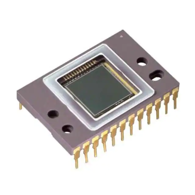
�KAF-3200
2184 (H) x 1472 (V) Full
Frame CCD Image Sensor
Description
The KAF−3200 Image Sensor is a high performance CCD
(charge−coupled device) with 2184 (H) x 1472 (V) photoactive pixels
designed for a wide range of image sensing applications.
The sensor incorporates true two−phase CCD technology,
simplifying the support circuits required to drive the sensor as well as
reducing dark current without compromising charge capacity. The
sensor also utilizes the TRUESENSE Transparent Gate Electrode to
improve sensitivity compared to the use of a standard front side
illuminated polysilicon electrode.
www.onsemi.com
Table 1. GENERAL SPECIFICATIONS
Parameter
Typical Value
Architecture
Full Frame CCD
Total Number of Pixels
2184 (H) x 1510 (V)
Number of Active Pixels
2184 (H) x 1472 (V)
Pixel Size
6.8 mm (H) x 6.8 mm (V)
Active Imager Size
14.85 mm (H) x 10.26 mm (V)
18 mm (diag), 4/3” optical format
Optical Fill−Factor
100%
Saturation Signal
55,000 electrons
Output Sensitivity
12 mV/e−
Readout Noise (1 MHz)
7 electrons rms
Dark Current
(25°C, Accumulation Mode)
< 7 pA/cm2
Dark Current Doubling Rate
6°C
Dynamic Range
(Sat Sig / Dark Noise)
78 dB
Quantum Efficiency with microlenses
(Red, Green, Blue)
55%, 70%, 80%
Maximum Data Rate
15 MHz
Package
CERDIP Package (sidebrazed)
Cover Glass
Clear or AR coated, 2 sides
Figure 1. KAF−3200 CCD Image Sensor
March, 2015 − Rev. 3
• True Two Phase Full Frame Architecture
• TRUESENSE Transparent Gate Electrode
•
•
•
•
for High Sensitivity
100% Fill Factor
Low Dark Current
Microlenses
High Output Sensitivity
Applications
• Medical Imaging
• Scientific Imaging
NOTE: Parameters above are specified at T = 25°C unless otherwise noted.
© Semiconductor Components Industries, LLC, 2015
Features
1
ORDERING INFORMATION
See detailed ordering and shipping information on page 2 of
this data sheet.
Publication Order Number:
KAF−3200/D
�KAF−3200
ORDERING INFORMATION
Table 2. ORDERING INFORMATION
Part Number
Description
Marking Code
KAF−3200−ABA−CD−B2
Monochrome, Telecentric Microlens, CERDIP Package (sidebrazed),
Clear Cover Glass with AR coating (both sides), Grade 2
KAF−3200−ABA
(Serial Number)
KAF−3200−ABA−CD−AE
Monochrome, Telecentric Microlens, CERDIP Package (sidebrazed),
Clear Cover Glass with AR coating (both sides), Engineering Sample
KAF−3200−ABA−CP−B2
Monochrome, Telecentric Microlens, CERDIP Package (sidebrazed),
Taped Clear Cover Glass, no coatings, Grade 2
KAF−3200−ABA−CP−AE
Monochrome, Telecentric Microlens, CERDIP Package (sidebrazed),
Taped Clear Cover Glass, no coatings, Engineering Sample
KAF−3200−12−5−A−EVK
Evaluation Board (Complete Kit)
KAF−3200−ABA
(Serial Number)
N/A
See the ON Semiconductor Device Nomenclature document (TND310/D) for a full description of the naming convention
used for image sensors. For reference documentation, including information on evaluation kits, please visit our web site at
www.onsemi.com.
www.onsemi.com
2
�KAF−3200
DEVICE DESCRIPTION
Architecture
4 Dark line
ϕV1
= scavanging CCDs
to reduce edge
artifacts
ϕV2
KAF − 3200
Usable Active Area:
2184(H) x 1472(V)
6.8 mm x 6.8 mm pixels
Vrd
ϕR
Vdd
Vout
Vss
Vlg
Sub
Vog
34 Dark line
2184 Active Pixels/Line
34 Dark
34 Dark
ϕH1
ϕH2
1 active(CTE monitor)
3 Invalid
1 active(CTE monitor)
8 Invalid
2 Invalid
Figure 2. Block Diagram
Dark Reference Pixels
The sensor is built with a true two−phase CCD technology
employing a transparent gate and with microlenses
available. This technology simplifies the support circuits
that drive the sensor and reduces the dark current without
compromising charge capacity. The transparent gate results
in spectral response increased ten times at 400 nm,
compared to a front side illuminated standard poly silicon
gate technology. The micro lenses are an integral part of each
pixel and cause most of the light to pass through the
transparent gate half of the pixel, further improving the
spectral sensitivity.
The photoactive area is 14.85 mm x 10.26 mm and is
housed in a 24 pin, dual in line (DIP) package with 0.1” pin
spacing.
The sensor consists of 2254 parallel (vertical) CCD shift
registers each 1510 elements long. These registers act as
both the photosensitive elements and as the transport circuits
that allow the image to be sequentially read out of the sensor.
The parallel (vertical) CCD registers transfer the image one
line at a time into a single 2267 element (horizontal) CCD
shift register. The horizontal register transfers the charge to
a single output amplifier. The output amplifier is a two−stage
source follower that converts the photo−generated charge to
a voltage for each pixel.
At the beginning of each line are 34 light shielded pixels.
There are also 34 full dark lines at the start of every frame
and 4 full dark lines at the end of each frame. Under normal
circumstances, the pixels in these dark lines do not respond
to light. However, dark reference pixels in close proximity
to an active pixel, (including the 2 full dark lines and one
column at end of each line), can scavenge signal depending
on light intensity and wavelength and therefore will not
represent the true dark signal.
Output Structure
Charge presented to the floating diffusion (FD) is
converted into a voltage and current amplified in order to
drive off−chip loads. The resulting voltage change seen at
the output is linearly related to the amount of charge placed
on FD. Once the signal has been sampled by the system
electronics, the reset gate (ϕR) is clocked to remove the
signal and FD is reset to the potential applied by VRD. More
signal at the floating diffusion reduces the voltage seen at the
output pin. In order to activate the output structure, an
off−chip load must be added to the Vout pin of the device.
See Figure 3.
www.onsemi.com
3
�KAF−3200
Charge Transport
Transfer Efficiency Test Pixels and Dummy Pixels
At the beginning of each line and at the end of each line
are extra horizontal CCD pixels. These are a combination of
pixels that are not associated with any vertical CCD register
and two that are associated with extra photoactive vertical
CCDs. These are provided to give an accurate
photosensitive signal that can be used to monitor the charge
transfer efficiency in the serial (horizontal) register.
They are arranged as follows beginning with the first pixel
in each line.
• 8 dark, inactive pixels
• 1 photoactive
• 3 inactive pixels
• 34 dark reference pixels
• 2184 photoactive pixels
• 34 dark pixels
• 1 photo active pixel
• 2 inactive pixels
Referring to Figure 8, the integrated charge from each
photo−gate is transported to the output using a two−step
process. Each line (row) of charge is first transported from
the vertical CCDs to the horizontal CCD register using the
ϕV1 and ϕV2 register clocks. The horizontal CCD is
presented a new line on the falling edge of ϕV1 while ϕH2
is held high. The horizontal CCD’s then transport each line,
pixel by pixel, to the output structure by alternately clocking
the ϕH1 and ϕH2 pins in a complementary fashion. On each
falling edge of ϕH1 a new charge packet is transferred onto
a floating diffusion and sensed by the output amplifier.
Horizontal Register
Output Structure
+15 V
0.1 mF
∼ 5 ma
Vout
2N3904 or equivalent
Image Acquisition
Buffered Output
An electronic representation of an image is formed when
incident photons falling on the sensor plane create
electron−hole pairs within the sensor. These
photon−induced electrons are collected locally by the
formation of potential wells at each pixel site. The number
of electrons collected is linearly dependent on light level and
exposure time, and non−linearly dependent on wavelength.
When the pixel’s capacity is reached, excess electrons will
leak into the adjacent pixels within the same column. This
is termed blooming. During the integration period, the ϕV1
and ϕV2 register clocks are held at a constant (low) level.
See Figure 7.
R1 = 140 W
1 kW
Figure 3. Output Structure Load Diagram
Notes:
1. For Operation of up to 10 MHz.
2. The value of R1 depends on the desired output
current according the following formula:
R1 = 0.7 / Iout
3. The optimal output current depends on the
capacitance that needs to be driven by the
amplifier and the bandwidth required. 5 mA is
recommended for capacitance of 12 pF and pixel
rates up to 15 MHz.
www.onsemi.com
4
�KAF−3200
PHYSICAL DESCRIPTION
Pin Description and Device Orientation
Pin 1
24 N/C
VOG
1
VOUT
2
VDD
3
22 ϕV1
VRD
4
21 ϕV1
ϕR
5
20 ϕV2
VSS
6
19 ϕV2
ϕH1
7
18 ϕV2
ϕH2
8
17 ϕV2
N/C
9
16 ϕV1
N/C
10
15 ϕV1
N/C
11
14 VSUB
VSUB
12
13 VSUB
23 VGUARD
Pixel 1,1
Figure 4. Pinout Diagram
NOTE: The KAF−3200 is designed to be compatible with the KAF−1602 and KAF−0401 series of Image sensors.
The exception is the addition of two new Vsub connections on pins 12 and 13.
Table 3. PIN DESCRIPTION
Pin
Name
Output Gate
24
N/C
Video Output
23
VGUARD
VDD
Amplifier Supply
22
ϕV1
Vertical CCD Clock − Phase 1
4
VRD
Reset Drain
21
ϕV1
Vertical CCD Clock − Phase 1
5
ϕR
Reset Clock
20
ϕV2
Vertical CCD Clock − Phase 2
ϕV2
Vertical CCD Clock − Phase 2
Pin
Name
1
VOG
2
VOUT
3
Description
Description
No Connection (open pin)
Substrate (Ground)
6
VSS
Amplifier Supply Return
19
7
ϕH1
Horizontal CCD Clock − Phase 1
18
ϕV2
Vertical CCD Clock − Phase 2
8
ϕH2
Horizontal CCD Clock − Phase 2
17
ϕV2
Vertical CCD Clock − Phase 2
9
N/C
No Connection (open pin)
16
ϕV1
Vertical CCD Clock − Phase 1
10
N/C
No Connection (open pin)
15
ϕV1
Vertical CCD Clock − Phase 1
11
N/C
No Connection (open pin)
14
VSUB
Substrate (Ground)
Substrate (Ground)
13
VSUB
Substrate (Ground)
12
VSUB
www.onsemi.com
5
�KAF−3200
IMAGING PERFORMANCE
Typical Operational Conditions
All values measured at 25°C, and nominal operating conditions. These parameters exclude defective pixels.
Table 4. SPECIFICATIONS
Description
Saturation Signal
Vertical CCD Capacity
Horizontal CCD Capacity
Output Node Capacity
Symbol
Min
Nom.
50,000
100,000
100,000
55,000
110,000
110,000
Max
Nsat
Quantum Efficiency with Microlenses
Red
Blue
Green
Verification
Plan
e−/pixel
1
design11
%QE
3
design11
design11
design11
55
70
80
PRNL
1
2
Photoresponse Non−Uniformity
PRNU
1
3
Jdark
Dark Signal Doubling Temperature
Dark Signal Non−Uniformity
Notes
120,000
Photoresponse Non−Linearity
Dark Signal
Units
5
DSNU
%
2
design11
%
3
die10
4
die10
e−/
15
6
30
10
6
7
°C
15
30
e−/ pixel / s
5
die10
dB
6
design118
Dynamic Range
DR
72
77
Charge Transfer Efficiency
CTE
0.99997
0.99999
Output Amplifier DC Offset
Vodc
Vrd − 2
Vrd − 1
Output Amplifier Bandwidth
f−3dB
Output Amplifier Sensitivity
Vout/ne−
Output Amplifier Output Impedance
Zout
Noise Floor
ne−
pixel / s
pA/cm2
design11
die10
V
7
die10
45
MHz
8
design11
18
20
mV/e−
design11
175
200
250
W
design11
7
12
electrons
Vrd
9
die10
1. For pixel binning applications, electron capacity up to 150,000 can be achieved with modified CCD inputs. Each sensor may have to be
optimized individually for these applications. Some performance parameters may be compromised to achieve the largest signals.
2. Worst case deviation from straight line fit, between 2% and 90% of Nsat.
3. One Sigma deviation of a 128 x 128 sample when CCD illuminated uniformly.
4. Average of all pixels with no illumination at 25°C.
5. Average dark signal of any of 11 x 8 blocks within the sensor. (Each block is 128 x 128 pixels)
6. 20log (Nsat / ne−) at nominal operating frequency and 25°C.
7. Video level offset with respect to ground.
8. Last output amplifier stage only. Assumes 10 pF off−chip load.
9. Output noise at −10°C, 1 MHz operating frequency (15 MHz bandwidth), and tint = 0 (excluding dark signal).
10. A parameter that is measured on every sensor during production testing.
11. A parameter that is quantified during the design verification activity.
www.onsemi.com
6
�KAF−3200
TYPICAL PERFORMANCE CURVES
KAF−3200 Spectral Response
Figure 5. Typical Spectral Response
www.onsemi.com
7
�KAF−3200
DEFECT DEFINITIONS
Operating Conditions
All defect tests performed at T = 25°C.
Table 5. SPECIFICATIONS
Point Defect
Classification
C2
Cluster Defect
Column Defect
Total
Zone A
Total
Zone A
Total
Zone A
≤ 10
≤5
≤4
≤2
0
0
1,1472
2184, 1472
320,1256
1864,1256
Zone A
1864,216
320, 216
1,1
2184, 1
Zone A = Central 1544H x 1040V Region
Figure 6. Active Pixel Region
Point Defects
Dark: A pixel that deviates by more than 6% from
neighboring pixels when illuminated to 70% of saturation.
−or−
Bright: A pixel with a dark current greater than
15000 e−/pixel/sec at 25°C.
Column Defect
A grouping of > 5 contiguous point defects along a single
column.
A column containing a pixel with dark current
> 12,000 e−/pixel/sec (bright column).
−or−
A column column that does not meet the minimum
vertical CCD charge capacity (low charge capacity column).
−or−
A column which loses more than 250 e− under 2 ke−
illumination (trap defect).
Cluster Defect
A grouping of not more than 5 adjacent point defects.
Neighboring Pixels
The surrounding 128 x 128 pixels or ±64 column/rows.
Defect Separation
Column and cluster defects are separated by no less than
two (2) pixels in any direction (excluding single pixel
defects).
www.onsemi.com
8
�KAF−3200
OPERATION
Table 6. ABSOLUTE MAXIMUM RATINGS
Description
Symbol
Minimum
Maximum
Units
Notes
Diode Pin Voltages
Vdiode
0
20
V
1, 2
Gate Pin Voltages − Type 1
Vgate1
−16
16
V
1, 3
Gate Pin Voltages − Type 2
Vgate2
0
16
V
1, 4
Inter−Gate Voltages
Vg−g
16
V
5
Output Bias Current
Iout
−10
mA
6
Cload
15
pF
6
Output Load Capacitance
Operating Temperature
TOP
−60
60
°C
Humidity
RH
5
90
%
7
Stresses exceeding those listed in the Maximum Ratings table may damage the device. If any of these limits are exceeded, device functionality
should not be assumed, damage may occur and reliability may be affected.
1. Referenced to pin SUB.
2. Includes pins: VRD, VDD, VSS, VOUT.
3. Includes pins: ϕV1, ϕV2, ϕH1, ϕH2.
4. Includes pins: VOG, ϕR.
5. Voltage difference between overlapping gates. Includes: ϕV1 to ϕV2, ϕH1 to ϕH2, ϕV2 to ϕH1, ϕH2 to VOG.
6. Avoid shorting output pins to ground or any low impedance source during operation.
7. T = 25°C. Excessive humidity will degrade MTTF.
Table 7. DC BIAS OPERATING CONDITIONS
Description
Reset Drain
Symbol
Minimum
Nominal
Maximum
Units
Maximum DC
Current (mA)
VRD
11.0
12.0
12.25
V
0.01
Output Amplifier Return
VSS
2.5
3.0
3.2
V
−0.5
Output Amplifier Supply
VDD
14.5
15.0
15.25
V
IOUT
Substrate
VSUB
0
0
0
V
0.01
Output Gate
VOG
4.75
5.0
5.5
V
0.01
VGUARD
9.0
10.0
12.0
V
−5.0
−10.0
mA
Guard
Video Output Current
IOUT
Notes
1
1. An output load sink must be applied to Vout to activate output amplifier – see Figure 3.
AC Operating Conditions
Table 8. CLOCK LEVELS
Symbol
Level
Minimum
Nominal
Maximum
Units
Effective
Capacitance
Vertical CCD Clock − Phase 1
ϕV1
Low
−10.0
−8.5
−8.5
V
5 nF (all ϕV1 pins)
Vertical CCD Clock − Phase 1
ϕV1
High
0.0
2.0
3.0
V
5 nF (all ϕV1 pins)
Vertical CCD Clock − Phase 2
ϕV2
Low
−10.0
−8.5
−8.5
V
5 nF (all ϕV2 pins)
Vertical CCD Clock − Phase 2
ϕV2
High
0.0
2.0
3.0
V
5 nF (all ϕV2 pins)
Horizontal CCD Clock − Phase 1
ϕH1
Low
−3.5
−3.0
−2.0
V
150 pF
Horizontal CCD Clock − Phase 1
ϕH1
High
ϕH1 Low + 10
7.0
ϕH1 Low + 10
V
150 pF
Horizontal CCD Clock − Phase 2
ϕH2
Low
−3.5
−3.0
−2.0
V
150 pF
Horizontal CCD Clock − Phase 2
ϕH2
High
ϕH2 Low + 10
7.0
ϕH2 Low + 10
V
150 pF
Reset Clock
ϕR
Low
3.0
4.0
4.25
V
5 pF
Reset Clock
ϕR
High
10.0
11.0
11.25
V
5 pF
Description
1. All pins draw less than 10 mA DC current.
www.onsemi.com
9
�KAF−3200
TIMING
Table 9. REQUIREMENTS AND CHARACTERISTICS
Description
Symbol
Minimum
Nominal
Maximum
Units
Notes
10
12
MHz
1, 2, 3
ϕH1, ϕH2 Clock Frequency
fH
Pixel Period (1 count)
te
67
100
ns
ϕH1, ϕH2 Setup Time
tϕHS
0.5
1
ms
ϕV1, ϕV2 Clock Pulse Width
tϕV
4
5
ms
2
Reset Clock Pulse Width
tϕR
5
20
ns
4
treadout
252.5
366.3
ms
5
Readout Time
Integration Time
tint
Line Time
tline
6
167.2
242.6
7
ms
1. 50% duty cycle values.
2. CTE may degrade above the nominal frequency.
3. Rise and fall times (10/90% levels) should be limited to 5−10% of clock period. Cross−over of register clocks should be between 40−60%
of amplitude.
4. ϕR should be clocked continuously.
5. treadout = (1510 * tline)
6. Integration time is user specified. Longer integration times will degrade noise performance due to dark signal fixed pattern and shot noise.
7. tline = (3 * tϕV) + tϕHS + (2267) + te−
Frame Timing
tint
tReadout
1 Frame = 1510 Lines
ϕV1
Line
1
2
ϕV2
ϕH1
ϕH2
Figure 7. Frame Timing
www.onsemi.com
10
1509
1510
�KAF−3200
Line Timing (Each Output)
Pixel Timing Detail
Line Timing Detail
tϕV
tϕR
ϕR
ϕV1
tϕV
1 line
ϕH1
ϕV2
te
tϕHS
te
1 count
ϕH2
ϕH1
Vpix
ϕH2
Vout
2267 counts
Vsat
Vdark
ϕR
Vodc
Vsub
Figure 8. Line Timing
Line Content
1−12
13−46
47 − 2230
Photoactive Pixels
Vsat
Vdark
Vpix
2231−2264 2265−2267 Vodc
Vsub
Dummy Pixels
Saturated pixel video output signal
Video output signal in no light situation, not zero due to Jdark
Pixel video output signal level, more electrons =more negative*
Video level offset with respect to vsub
Analog Ground
* See Image Aquisition section (page 4)
Dark Reference Pixels
Figure 9. Timing Diagrams
NOTE: The KAF−3200 was designed to be compatible with the KAF−1602 and KAF−0401 series of image sensors.
Please note that the polarities of the two−phase clocks have been swapped on the KAF−3200 compared to the
KAF−1602 and KAF−0401.
www.onsemi.com
11
�KAF−3200
STORAGE AND HANDLING
Table 10. STORAGE CONDITIONS
Description
Symbol
Minimum
Maximum
Units
Notes
Storage Temperature
TST
−20
80
°C
1
Humidity
RH
5
90
%
2
1. Storage toward the maximum temperature will accelerate color filter degradation.
2. T = 25°C. Excessive humidity will degrade MTTF.
For information on ESD and cover glass care and
cleanliness, please download the Image Sensor Handling
and Best Practices Application Note (AN52561/D) from
www.onsemi.com.
For quality and reliability information, please download
the Quality & Reliability Handbook (HBD851/D) from
www.onsemi.com.
For information on device numbering and ordering codes,
please download the Device Nomenclature technical note
(TND310/D) from www.onsemi.com.
For information on soldering recommendations, please
download the Soldering and Mounting Techniques
Reference
Manual
(SOLDERRM/D)
from
www.onsemi.com.
For information on Standard terms and Conditions of
Sale, please download Terms and Conditions from
www.onsemi.com.
www.onsemi.com
12
�KAF−3200
MECHANICAL INFORMATION
Completed Assembly
Figure 10. Completed Assembly (1 of 2)
www.onsemi.com
13
�KAF−3200
Figure 11. Completed Assembly (2 of 2)
www.onsemi.com
14
�KAF−3200
AR Cover Glass Transmission
%Transmission of AR Cover Glass
100
90
80
% Transmission
70
60
50
40
30
20
10
0
300
400
500
600
700
800
900
Wavelength (nm)
Figure 12. Antireflective Cover Glass Transmission
ON Semiconductor and the
are registered trademarks of Semiconductor Components Industries, LLC (SCILLC) or its subsidiaries in the United States and/or other countries.
SCILLC owns the rights to a number of patents, trademarks, copyrights, trade secrets, and other intellectual property. A listing of SCILLC’s product/patent coverage may be accessed
at www.onsemi.com/site/pdf/Patent−Marking.pdf. SCILLC reserves the right to make changes without further notice to any products herein. SCILLC makes no warranty, representation
or guarantee regarding the suitability of its products for any particular purpose, nor does SCILLC assume any liability arising out of the application or use of any product or circuit, and
specifically disclaims any and all liability, including without limitation special, consequential or incidental damages. “Typical” parameters which may be provided in SCILLC data sheets
and/or specifications can and do vary in different applications and actual performance may vary over time. All operating parameters, including “Typicals” must be validated for each
customer application by customer’s technical experts. SCILLC does not convey any license under its patent rights nor the rights of others. SCILLC products are not designed, intended,
or authorized for use as components in systems intended for surgical implant into the body, or other applications intended to support or sustain life, or for any other application in which
the failure of the SCILLC product could create a situation where personal injury or death may occur. Should Buyer purchase or use SCILLC products for any such unintended or
unauthorized application, Buyer shall indemnify and hold SCILLC and its officers, employees, subsidiaries, affiliates, and distributors harmless against all claims, costs, damages, and
expenses, and reasonable attorney fees arising out of, directly or indirectly, any claim of personal injury or death associated with such unintended or unauthorized use, even if such claim
alleges that SCILLC was negligent regarding the design or manufacture of the part. SCILLC is an Equal Opportunity/Affirmative Action Employer. This literature is subject to all applicable
copyright laws and is not for resale in any manner.
PUBLICATION ORDERING INFORMATION
LITERATURE FULFILLMENT:
Literature Distribution Center for ON Semiconductor
P.O. Box 5163, Denver, Colorado 80217 USA
Phone: 303−675−2175 or 800−344−3860 Toll Free USA/Canada
Fax: 303−675−2176 or 800−344−3867 Toll Free USA/Canada
Email: orderlit@onsemi.com
N. American Technical Support: 800−282−9855 Toll Free
USA/Canada
Europe, Middle East and Africa Technical Support:
Phone: 421 33 790 2910
Japan Customer Focus Center
Phone: 81−3−5817−1050
www.onsemi.com
15
ON Semiconductor Website: www.onsemi.com
Order Literature: http://www.onsemi.com/orderlit
For additional information, please contact your local
Sales Representative
KAF−3200/D
�