KSH42C
KSH42C
General Purpose Amplifier
Low Speed Switching Applications
• Lead Formed for Surface Mount Application (No Suffix)
• Straight Lead (I-PAK, “- I” Suffix)
• Electrically Similar to Popular TIP42C
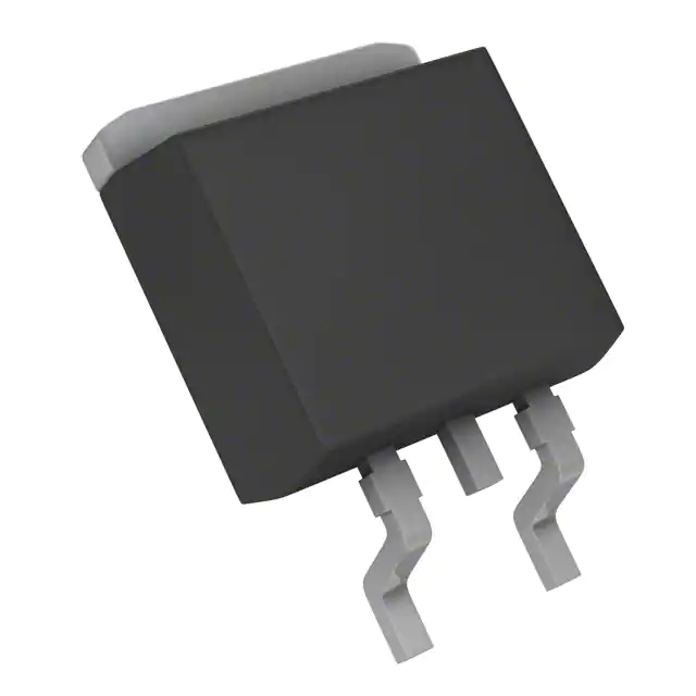
D-PAK
1
1.Base
I-PAK
1
2.Collector
3.Emitter
PNP Epitaxial Silicon Transistor
Absolute Maximum Ratings TC=25°C unless otherwise noted
Symbol
VCBO
Parameter
Value
-100
Collector-Base Voltage
VCEO
Collector-Emitter Voltage
VEBO
Emitter-Base Voltage
IC
Collector Current (DC)
ICP
Collector Current (Pulse)
Units
V
-100
V
-5
V
-6
A
-10
A
IB
Base Current
-2
A
PC
Collector Dissipation (TC=25°C)
20
W
Collector Dissipation (Ta=25°C)
1.75
W
TJ
Junction Temperature
150
°C
TSTG
Storage Temperature
- 65 ~ 150
°C
Electrical Characteristics TC=25°C unless otherwise noted
Symbol
VCEO(sus)
Parameter
* Collector-Emitter Sustaining Voltage
Test Condition
IC = - 30mA, IB = 0
ICEO
Collector Cut-off Current
ICES
Collector Cut-off Current
IEBO
Min.
-100
Max.
Units
V
VCE = -60V, IB = 0
-50
µA
VCE = -100V, VBE = 0
-10
µA
Emitter Cut-off Current
VBE = -5V, IC = 0
-0.5
mA
hFE
* DC Current Gain
VCE = -4V, IC = -0.3A
VCE = -4V, IC = -3A
VCE(sat)
* Collector-Emitter Saturation Voltage
IC = -6A, IB = -600mA
VBE(on)
* Base-Emitter On Voltage
VCE = -6A, IC = -4A
fT
Current Gain Bandwidth Product
VCE = -10V, IC = -500mA
30
15
3
75
-1.5
V
-2
V
MHz
* Pulse Test: PW≤300µs, Duty Cycle≤2%
©2002 Semiconductor Components Industries, LLC.
October-2017,Rev. 1
Publication Order Number:
KSH42C/D
�KSH42C
VBE(sat), VCE(sat)[V], SATURATION VOLTAGE
Typical Characteristics
1000
hFE, DC CURRENT GAIN
VCE = -2V
100
10
1
-0.01
-0.1
-1
-10
-10
IC = 10 IB
-1
V BE(sat)
-0.1
VCE(sat)
-0.01
-0.01
-0.1
-1
-10
IC[A], COLLECTOR CURRENT
IC[A], COLLECTOR CURRENT
Figure 1. DC current Gain
Figure 2. Base-Emitter Saturation Voltage
Collector-Emitter Saturation Voltage
10
tR, tD [µs], TURN ON TIME
Cob[pF], CAPACITANCE
1000
100
10
V CC = -30V
IC = 10.IB
1
tR
0.1
tD VBE(off)=-5V
1
-0.1
0.01
-0.01
-1
-10
-0.1
-10
IC[A], COLLECTOR CURRENT
VCB[V], COLLECTOR-BASE VOLTAGE
Figure 3. Collector Capacitance
Figure 4. Turn On Time
10
-100
V CC = -30V
IC = 10.IB
tSTG
1
tF
0.1
0.01
-0.01
IC[A], COLLECTOR CURRENT
tSTG,tF [µ s], TURN OFF TIME
-1
-100
-0.1
-1
-10
ICP(max)
-10
10
1m
IC(max)
5m
-1
50
s
0µ
0µ
s
s
s
DC
-0.1
-0.01
-1
IC[A], COLLECTOR CURRENT
-10
-100
VCE[V], COLLECTOR-EMITTER VOLTAGE
Figure 5. Turn Off Time
Figure 6. Safe Operating Area
www.onsemi.com
2
-1000
�KSH42C
Typical Characteristics (Continued)
PC[W], POWER DISSIPATION
25
20
15
10
5
0
0
25
50
75
100
125
150
175
o
TC[ C], CASE TEMPERATURE
Figure 7. Power Derating
www.onsemi.com
3
�KSH42C
Package Dimensions
D-PAK
MIN0.55
0.91 ±0.10
0.50 ±0.10
0.89 ±0.10
0.50 ±0.10
1.02 ±0.20
2.30TYP
[2.30±0.20]
(1.00)
(3.05)
(2XR0.25)
(0.10)
6.60 ±0.20
(5.34)
(5.04)
(1.50)
(0.70)
2.30 ±0.20
(0.90)
6.10 ±0.20
2.70 ±0.20
2.30 ±0.10
0.76 ±0.10
6.10 ±0.20
2.30TYP
[2.30±0.20]
(0.50)
2.70 ±0.20
MAX0.96
(4.34)
9.50 ±0.30
0.80 ±0.20
0.60 ±0.20
(0.50)
9.50 ±0.30
5.34 ±0.30
0.70 ±0.20
6.60 ±0.20
0.76 ±0.10
Dimensions in Millimeters
www.onsemi.com
4
�KSH42C
Package Dimensions (Continued)
I-PAK
2.30 ±0.20
6.60 ±0.20
5.34 ±0.20
2.30TYP
[2.30±0.20]
±0.20
±0.30
16.10
±0.20
±0.30
9.30
0.76 ±0.10
1.80
0.80
MAX0.96
0.50 ±0.10
6.10
±0.20
(0.50)
0.70
(4.34)
±0.10
0.60
±0.20
(0.50)
2.30TYP
[2.30±0.20]
0.50 ±0.10
Dimensions in Millimeters
www.onsemi.com
5
�ON Semiconductor and
are trademarks of Semiconductor Components Industries, LLC dba ON Semiconductor or its subsidiaries in the United States and/or other countries.
ON Semiconductor owns the rights to a number of patents, trademarks, copyrights, trade secrets, and other intellectual property. A listing of ON Semiconductor’s product/patent
coverage may be accessed at www.onsemi.com/site/pdf/Patent−Marking.pdf. ON Semiconductor reserves the right to make changes without further notice to any products herein.
ON Semiconductor makes no warranty, representation or guarantee regarding the suitability of its products for any particular purpose, nor does ON Semiconductor assume any liability
arising out of the application or use of any product or circuit, and specifically disclaims any and all liability, including without limitation special, consequential or incidental damages.
Buyer is responsible for its products and applications using ON Semiconductor products, including compliance with all laws, regulations and safety requirements or standards,
regardless of any support or applications information provided by ON Semiconductor. “Typical” parameters which may be provided in ON Semiconductor data sheets and/or
specifications can and do vary in different applications and actual performance may vary over time. All operating parameters, including “Typicals” must be validated for each customer
application by customer’s technical experts. ON Semiconductor does not convey any license under its patent rights nor the rights of others. ON Semiconductor products are not
designed, intended, or authorized for use as a critical component in life support systems or any FDA Class 3 medical devices or medical devices with a same or similar classification
in a foreign jurisdiction or any devices intended for implantation in the human body. Should Buyer purchase or use ON Semiconductor products for any such unintended or unauthorized
application, Buyer shall indemnify and hold ON Semiconductor and its officers, employees, subsidiaries, affiliates, and distributors harmless against all claims, costs, damages, and
expenses, and reasonable attorney fees arising out of, directly or indirectly, any claim of personal injury or death associated with such unintended or unauthorized use, even if such
claim alleges that ON Semiconductor was negligent regarding the design or manufacture of the part. ON Semiconductor is an Equal Opportunity/Affirmative Action Employer. This
literature is subject to all applicable copyright laws and is not for resale in any manner.
PUBLICATION ORDERING INFORMATION
LITERATURE FULFILLMENT:
Literature Distribution Center for ON Semiconductor
19521 E. 32nd Pkwy, Aurora, Colorado 80011 USA
Phone: 303−675−2175 or 800−344−3860 Toll Free USA/Canada
Fax: 303−675−2176 or 800−344−3867 Toll Free USA/Canada
Email: orderlit@onsemi.com
❖
© Semiconductor Components Industries, LLC
N. American Technical Support: 800−282−9855 Toll Free
USA/Canada
Europe, Middle East and Africa Technical Support:
Phone: 421 33 790 2910
Japan Customer Focus Center
Phone: 81−3−5817−1050
ON Semiconductor Website: www.onsemi.com
Order Literature: http://www.onsemi.com/orderlit
For additional information, please contact your local
Sales Representative
www.onsemi.com
�